ZHCSL46D March 2020 – June 2021 LM62440-Q1
PRODUCTION DATA
- 1 特性
- 2 应用
- 3 说明
- 4 Revision History
- 5 Description (continued)
- 6 Device Comparison Table
- 7 Pin Configuration and Functions
- 8 Specifications
-
9 Detailed Description
- 9.1 Overview
- 9.2 Functional Block Diagram
- 9.3
Feature Description
- 9.3.1 EN Uses for Enable and VIN UVLO
- 9.3.2 MODE/SYNC Pin Operation
- 9.3.3 PGOOD Output Operation
- 9.3.4 Internal LDO, VCC UVLO, and BIAS Input
- 9.3.5 Bootstrap Voltage and VCBOOT-UVLO (CBOOT Pin)
- 9.3.6 Adjustable SW Node Slew Rate
- 9.3.7 Spread Spectrum
- 9.3.8 Soft Start and Recovery From Dropout
- 9.3.9 Output Voltage Setting
- 9.3.10 Overcurrent and Short Circuit Protection
- 9.3.11 Thermal Shutdown
- 9.3.12 Input Supply Current
- 9.4 Device Functional Modes
-
10Application and Implementation
- 10.1 Application Information
- 10.2
Typical Application
- 10.2.1 Design Requirements
- 10.2.2
Detailed Design Procedure
- 10.2.2.1 Choosing the Switching Frequency
- 10.2.2.2 Setting the Output Voltage
- 10.2.2.3 Inductor Selection
- 10.2.2.4 Output Capacitor Selection
- 10.2.2.5 Input Capacitor Selection
- 10.2.2.6 BOOT Capacitor
- 10.2.2.7 BOOT Resistor
- 10.2.2.8 VCC
- 10.2.2.9 BIAS
- 10.2.2.10 CFF and RFF Selection
- 10.2.2.11 External UVLO
- 10.2.3 Application Curves
- 11Power Supply Recommendations
- 12Layout
- 13Device and Documentation Support
- 14Mechanical, Packaging, and Orderable Information
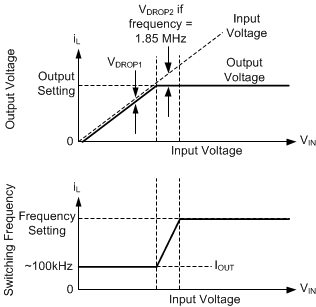
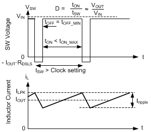
9.4.3.5 Dropout
Dropout operation is defined as any input-to-output voltage ratio that requires frequency to drop to achieve the required duty cycle. At a given clock frequency, duty cycle is limited by minimum off-time. Once this limit is reached, if clock frequency were maintained, output voltage would fall. Instead of allowing the output voltage to drop, the LM62440-Q1 extends on-time past the end of the clock cycle until needed peak inductor current is achieved. The clock is allowed to start a new cycle once peak inductor current is achieved or once a pre-determined maximum on-time, tON_MAX, of approximately 9 µs passes. As a result, once the needed duty cycle cannot be achieved at the selected clock frequency due to the existence of a minimum off-time, frequency drops to maintain regulation. If input voltage is low enough so that output voltage cannot be regulated even with an on-time of tON_MAX, output voltage drops to slightly below the input voltage, VDROP1. For additional information on recovery from dropout, reference Figure 9-16.

