ZHCSLU1B October 2022 – August 2024 LM64440-Q1 , LM64460-Q1
PRODUCTION DATA
- 1
- 1 特性
- 2 应用
- 3 说明
- 4 Device Comparison Table
- 5 Pin Configuration and Functions
- 6 Specifications
-
7 Detailed Description
- 7.1 Overview
- 7.2 Functional Block Diagram
- 7.3
Feature Description
- 7.3.1 Input Voltage Range (VIN1, VIN2)
- 7.3.2 Output Voltage Setpoint (FB)
- 7.3.3 Precision Enable and Input Voltage UVLO (EN)
- 7.3.4 MODE/SYNC Operation
- 7.3.5 Clock Locking
- 7.3.6 Power-Good Monitor (PGOOD)
- 7.3.7 Bias Supply Regulator (VCC, BIAS)
- 7.3.8 Bootstrap Voltage and UVLO (CBOOT)
- 7.3.9 Spread Spectrum
- 7.3.10 Soft Start and Recovery From Dropout
- 7.3.11 Overcurrent and Short-Circuit Protection
- 7.3.12 Thermal Shutdown
- 7.3.13 Input Supply Current
- 7.4 Device Functional Modes
-
8 Application and Implementation
- 8.1 Application Information
- 8.2
Typical Applications
- 8.2.1 Design 1 – Automotive Synchronous 6A Buck Regulator at 2.1MHz
- 8.2.2
Design 2 – Automotive Synchronous 4A Buck Regulator at 2.1MHz
- 8.2.2.1 Design Requirements
- 8.2.2.2
Detailed Design Procedure
- 8.2.2.2.1 Custom Design With WEBENCH® Tools
- 8.2.2.2.2 Setting the Output Voltage
- 8.2.2.2.3 Choosing the Switching Frequency
- 8.2.2.2.4 Inductor Selection
- 8.2.2.2.5 Output Capacitor Selection
- 8.2.2.2.6 Input Capacitor Selection
- 8.2.2.2.7 Bootstrap Capacitor
- 8.2.2.2.8 VCC Capacitor
- 8.2.2.2.9 BIAS Power Connection
- 8.2.2.2.10 Feedforward Network
- 8.2.2.2.11 Input Voltage UVLO
- 8.2.2.3 Application Curves
- 8.3 Power Supply Recommendations
- 8.4 Layout
- 9 Device and Documentation Support
- 10Revision History
- 11Mechanical, Packaging, and Orderable Information
7.3.4.1 Level-Dependent MODE/SYNC Control
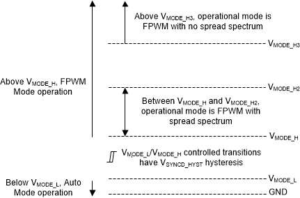
If only a single mode is used, configure the converter using level-dependent control. Note that the LM644x0-Q1 cannot be synchronized to an external clock signal in level-dependent mode. Table 7-1 shows a summary of level-dependent mode selection settings. The level-dependent mode selection setting registers after expiration of tMODE. Figure 7-2 also depicts a summary of the level-dependent modes.
| MODE/SYNC | MODE |
|---|---|
| Tie to GND | AUTO mode with spread spectrum |
| Tie to GND through 100kΩ | AUTO mode without spread spectrum |
| Tie to VCC or set VMODE_H < VMODE/SYNC < VMODE_H2 | FPWM mode with spread spectrum |
| Tie to VIN or set VMODE/SYNC > VMODE_H3 | FPWM mode without spread spectrum |
 Figure 7-2 Level-Dependent Mode Selection Settings
Note that during dropout operation, the input voltage is close to VCC. Because this condition is typically seen while operating in dropout, the switching frequency is typically folded back and spread spectrum is deactivated. When VIN increases and the device is no longer in frequency foldback, spread spectrum is reactivated. Also, when the input voltage is between 3V to 3.7V and the LM644x0-Q1 is not in dropout operation and spread spectrum operation is not assured.
One purpose of level-dependent MODE/SYNC pin control is to dynamically change between FPWM and AUTO modes. To make sure the resistance from MODE/SYNC to ground is less than RSYNC_L, use 6kΩ to ground. The MODE/SYNC pin can then be toggled between FPWM and AUTO modes as shown in Table 7-1.
If AUTO mode without spread spectrum operation is desired, tie MODE/SYNC to ground through a 100kΩ resistor. AUTO mode without spread spectrum is a fixed option, and the mode cannot be changed dynamically.