ZHCSFV1 December 2016 LM73-Q1
PRODUCTION DATA.
- 1 特性
- 2 应用
- 3 说明
- 4 修订历史记录
- 5 Pin Configuration and Functions
- 6 Specifications
- 7 Detailed Description
- 8 Application and Implementation
- 9 Power Supply Recommendations
- 10Layout
- 11器件和文档支持
- 12机械、封装和可订购信息
7 Detailed Description
7.1 Overview
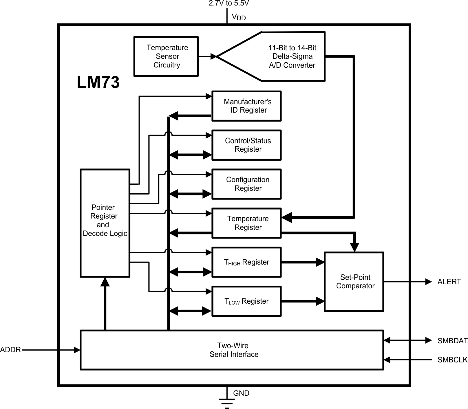
The LM73-Q1 is a digital temperature sensor that senses the temperature of its die using a sigma-delta analog-to-digital converter and stores the temperature in the Temperature Register. The LM73-Q1's 2-wire serial interface is compatible with SMBus 2.0 and I2C. Please see the SMBus 2.0 specification for a detailed description of the differences between the I2C bus and SMBus.
The temperature resolution is programmable, allowing the host system to select the optimal configuration between sensitivity and conversion time. The LM73-Q1 can be placed in shutdown to minimize power consumption when temperature data is not required. While in shutdown, a 1-shot conversion mode allows system control of the conversion rate for ultimate flexibility.
7.2 Functional Block Diagram
7.3 Feature Description
The LM73-Q1 features the following registers. See LM73-Q1 Registers for a complete list of the pointer address, content, and reset state of each register.
- Pointer Register
- Temperature Register
- Configuration Register
- THIGH Register
- TLOW Register
- Control/Status Register
- Identification Register
7.3.1 Power-On Reset
The power-on reset (POR) state is the point at which the supply voltage rises above the power-on reset threshold (specified in the Electrical Characteristics), generating an internal reset. Each of the registers contains a defined value upon POR and this data remains there until any of the following occurs:
- The first temperature conversion is completed, causing the Temperature Register and various status bits to be updated internally, depending on the value of the measured temperature.
- The master writes different data to any Read/Write (R/W) bits, or
- The LM73-Q1 is powered down.
7.3.2 One-Shot Conversion
The LM73-Q1 features a one-shot conversion bit, which is used to initiate a single conversion and comparison cycle when the LM73-Q1 is in shutdown mode. While the LM73-Q1 is in shutdown mode, writing a 1 to the One-Shot bit in the Configuration Register will cause the LM73-Q1 to perform a single temperature conversion and update the Temperature Register and the affected status bits. Operating the LM73-Q1 in this one-shot mode allows for extremely low average-power consumption, making it ideal for low-power applications.
When the One-Shot bit is set, the LM73-Q1 initiates a temperature conversion. After this initiation, but before the completion of the conversion and resultant register updates, the LM73-Q1 is in a "one-shot" state. During this state, the Data Available (DAV) flag in the Control/Status register is 0 and the Temperature Register contains the value 8000h (-256°C). All other registers contain the data that was present before initiating the one-shot conversion. After the temperature measurement is complete, the DAV flag will be set to 1 and the temperature register will contain the resultant measured temperature.
7.3.3 Temperature Data Format
The resolution of the temperature data and the size of the data word are user-selectable through bits RES1 and RES0 in the Control/Status Register. By default, the LM73-Q1 temperature stores the measured temperature in an 11-bit (10 bits plus sign) word with one least significant bit (LSB) equal to 0.25°C. The maximum word size is 14 bits (13-bits plus sign) with a resolution of 0.03125 °C/LSB.
| CONTROL BIT | DATA FORMAT | |||
|---|---|---|---|---|
| RES1 | RES0 | WORD SIZE | RESOLUTION | |
| 0 | 0 | 11 bits | 0.25 °C/LSB | |
| 0 | 1 | 12 bits | 0.125 °C/LSB | |
| 1 | 0 | 13 bits | 0.0625 °C/LSB | |
| 1 | 1 | 14 bits | 0.03125 °C/LSB | |
The temperature data is reported in 2's complement format. The word is stored in the 16-bit Temperature Register and is left justified in this register. Unused temperature-data bits are always reported as 0.
Table 1. 11-Bit (10-Bit Plus Sign)
| TEMPERATURE | DIGITAL OUTPUT | |
|---|---|---|
| BINARY | HEX | |
| 150°C | 0100 1011 0000 0000 | 4B00h |
| 25°C | 0000 1100 1000 0000 | 0C80h |
| 1°C | 0000 0000 1000 0000 | 0080h |
| 0.25°C | 0000 0000 0010 0000 | 0020h |
| 0°C | 0000 0000 0000 0000 | 0000h |
| −0.25°C | 1111 1111 1110 0000 | FFE0h |
| −1°C | 1111 1111 1000 0000 | FF80h |
| −25°C | 1111 0011 1000 0000 | F380h |
| −40°C | 1110 1100 0000 0000 | EC00h |
Table 2. 12-Bit (11-Bit Plus Sign)
| TEMPERATURE | DIGITAL OUTPUT | |
|---|---|---|
| BINARY | HEX | |
| 150°C | 0100 1011 0000 0000 | 4B00h |
| 25°C | 0000 1100 1000 0000 | 0C80h |
| 1°C | 0000 0000 1000 0000 | 0080h |
| 0.125°C | 0000 0000 0001 0000 | 0010h |
| 0°C | 0000 0000 0000 0000 | 0000h |
| −0.125°C | 1111 1111 1111 0000 | FFF0h |
| −1°C | 1111 1111 1000 0000 | FF80h |
| −25°C | 1111 0011 1000 0000 | F380h |
| −40°C | 1110 1100 0000 0000 | EC00h |
Table 3. 13-Bit (12-Bit Plus Sign)
| TEMPERATURE | DIGITAL OUTPUT | |
|---|---|---|
| BINARY | HEX | |
| 150°C | 0100 1011 0000 0000 | 4B00h |
| 25°C | 0000 1100 1000 0000 | 0C80h |
| 1°C | 0000 0000 1000 0000 | 0080h |
| 0.0625°C | 0000 0000 0000 1000 | 0008h |
| 0°C | 0000 0000 0000 0000 | 0000h |
| −0.0625°C | 1111 1111 1111 1000 | FFF8h |
| −1°C | 1111 1111 1000 0000 | FF80h |
| −25°C | 1111 0011 1000 0000 | F380h |
| −40°C | 1110 1100 0000 0000 | EC00h |
Table 4. 14-Bit (13-Bit Plus Sign)
| TEMPERATURE | DIGITAL OUTPUT | |
|---|---|---|
| BINARY | HEX | |
| 150°C | 0100 1011 0000 0000 | 4B00h |
| 25°C | 0000 1100 1000 0000 | 0C80h |
| 1°C | 0000 0000 1000 0000 | 0080h |
| 0.03125°C | 0000 0000 0000 0100 | 0004h |
| 0°C | 0000 0000 0000 0000 | 0000h |
| −0.03125°C | 1111 1111 1111 1100 | FFFCh |
| −1°C | 1111 1111 1000 0000 | FF80h |
| −25°C | 1111 0011 1000 0000 | F380h |
| −40°C | 1110 1100 0000 0000 | EC00h |
7.3.4 SMBus Interface
The LM73-Q1 operates as a slave on the SMBus. The SMBDAT line is bidirectional. The SMBCLK line is an input only. The LM73-Q1 never drives the SMBCLK line and it does not support clock stretching.
The LM73-Q1 uses a 7-bit slave address. It is available in two versions. Each version can be configured for one of three unique slave addresses, for a total of six unique address.
| PART NUMBER | ADDRESS PIN | DEVICE ADDRESS |
|---|---|---|
| LM73C0-Q1 | Float Ground VDD |
1001 000 1001 001 1001 010 |
| LM73C1-Q1 | Float Ground VDD |
1001 100 1001 101 1001 110 |
The SMBDAT output is an open-drain output and does not have internal pull-ups. A “high” level will not be observed on this pin until pull-up current is provided by some external source, typically a pull-up resistor. Choice of resistor value depends on many system factors but, in general, the pull-up resistor should be as large as possible without effecting the SMBus desired data rate. This will minimize any internal temperature reading errors due to internal heating of the LM73-Q1.
The LM73-Q1 features an integrated low-pass filter on both the SMBCLK and the SMBDAT line. These filters increase communications reliability in noisy environments.
If either the SMBCLK or SMBDAT line is held low for a time greater than tTIMEOUT (see Logic Electrical Characteristics for the value of tTIMEOUT), the LM73-Q1 state machine will reset to the SMBus idle state, releasing the data line. Once the SMBDAT is released high, the master may initiate an SMBus start.
7.3.5 ALERT Function
The ALERT output is an over-temperature indicator. At the end of every temperature conversion, the measured temperature is compared to the value in the THIGH Register. If the measured temperature exceeds the value stored in THIGH, the ALERT output goes active (see Figure 5). This over-temperature condition will also cause the ALRT_STAT bit in the Control/Status Register to change value (this bit mirrors the logic level of the ALERT pin).
The ALERT pin and the ALRT_STAT bit are cleared when any of the following occur:
- The measured temperature falls below the value stored in the TLOW Register
- A 1 is written to the ALERT Reset bit in the Configuration Register
- The master resets it through an SMBus Alert Response Address (ARA) procedure
If ALERT has been cleared by the master writing a 1 to the ALERT Reset bit, while the measured temperature still exceeds the THIGH setpoint, ALERT will go active again after the completion of the next temperature conversion.
Each temperature reading is associated with a Temperature High (THI) and a Temperature Low (TLOW) flag in the Control/Status Register. A digital comparison determines whether that reading is above the THIGH setpoint or below the TLOW setpoint. If so, the corresponding flag is set. All digital comparisons to the THIGH, and TLOW values are based on an 11-bit temperature comparison. Regardless of the resolution setting of the LM73-Q1, the lower three temperature LSBs will not affect the state of the ALERT output, THI flag, and TLOW flag.
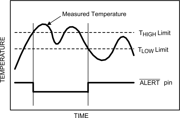 Figure 5. ALERT Temperature Response Cleared When Temperature Crosses TLOW
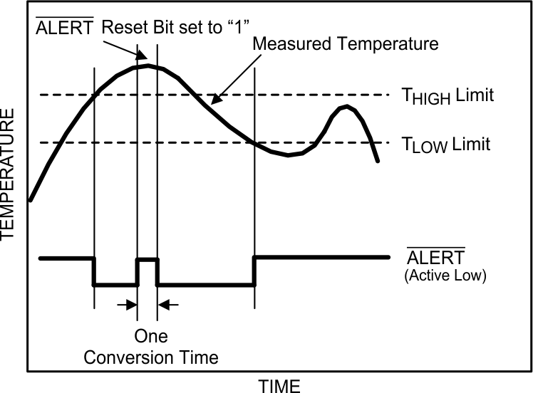 Figure 6. ALERT Temperature Response Cleared by Writing a 1 to the ALERT Reset Bit.
7.3.6 Communicating With the LM73-Q1
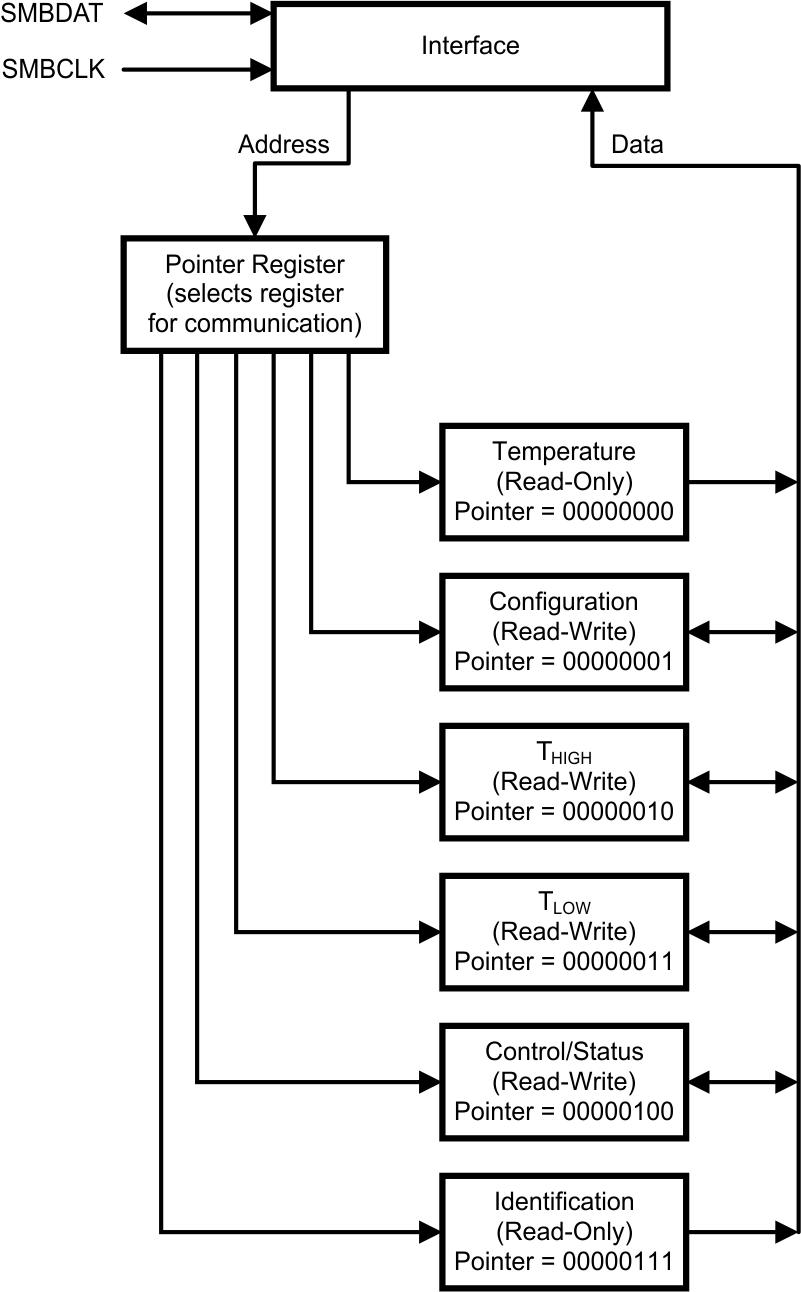
The data registers in the LM73-Q1 are selected by the Pointer Register. At power-up the Pointer Register is set to 00h, the location for the Temperature Register. The Pointer Register latches the last location it was set to. Note that all Pointer Register bits are decoded; any incorrect pointer values will not be acknowledged and will not be stored in the Pointer Register.
NOTE
A write to an invalid pointer address is not allowed. If the master writes an invalid address to the Pointer Register, the LM73-Q1 will not acknowledge the address and the Pointer Register will continue to contain the last value stored in it.
A Write to the LM73-Q1 will always include the address byte and the pointer byte.
A Read from the LM73-Q1 can occur in either of the following ways:
- If the location latched in the Pointer Register is correct (that is, the Pointer Register is pre-set prior to the read), then the read can simply consist of an address byte, followed by retrieving the data byte. Most of the time it is expected that the Pointer Register will point to Temperature Registers because that will be the data most frequently read from the LM73-Q1.
- If the Pointer Register needs to be set, then an address byte, pointer byte, repeat start, and another address byte will accomplish a read.
The data byte is read out of the LM73-Q1 by the most significant bit first. At the end of a read, the LM73-Q1 can accept either an Acknowledge or No Acknowledge bit from the Master. No Acknowledge is typically used as a signal to the slave that the Master has read its last byte.
7.3.6.1 Reading from the LM73-Q1
 Figure 7. Typical Read from a 2-Byte Register with Preset Pointer
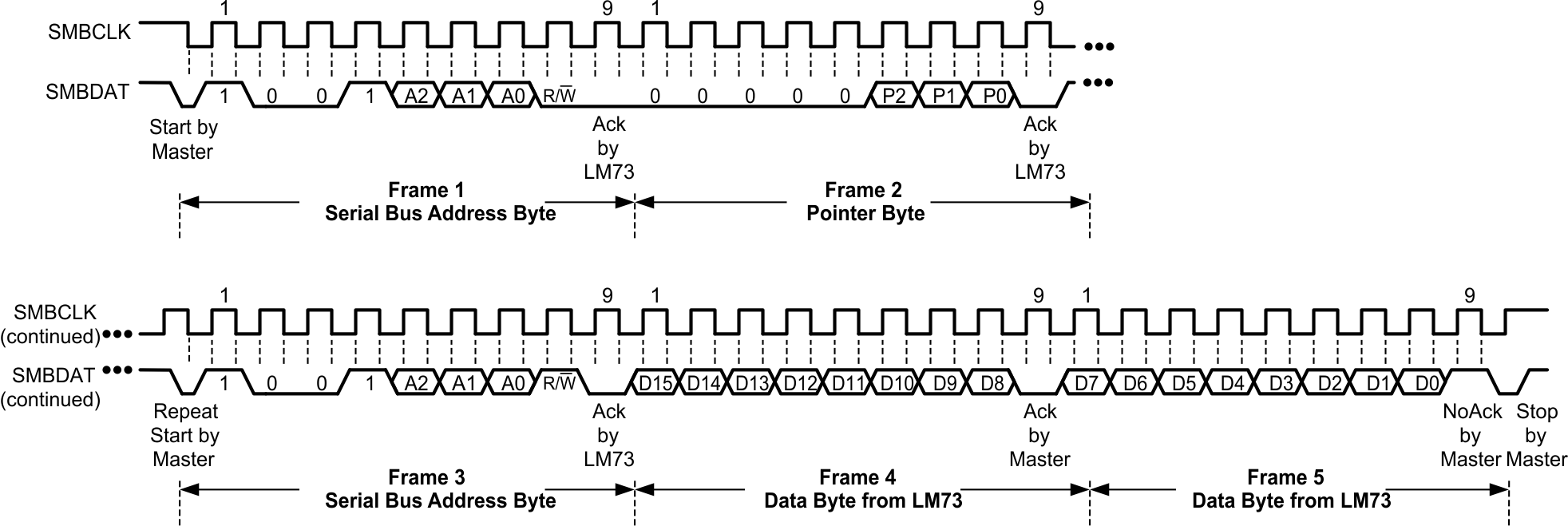 Figure 8. Typical Pointer Set Followed by Immediate Read of a 2-Byte Register
 Figure 9. Typical Read from a 1-Byte Register with Preset Pointer
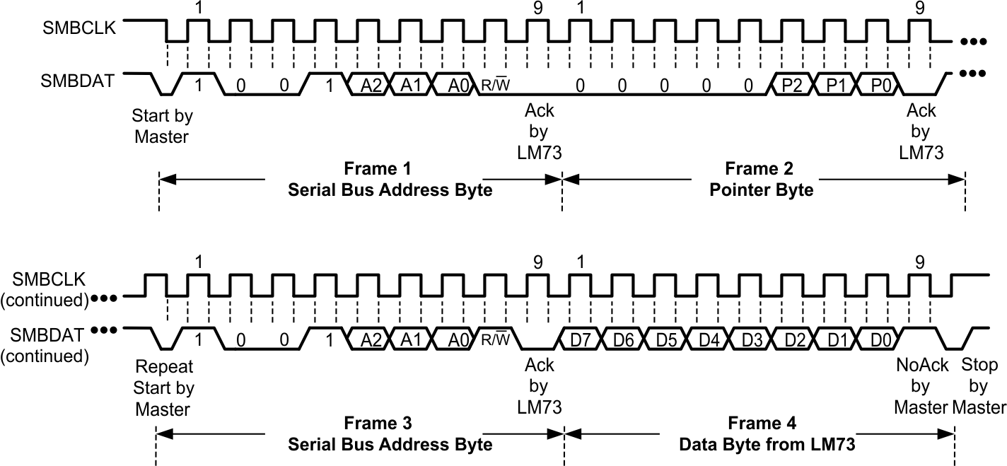 Figure 10. Typical Pointer Set Followed by Immediate Read of a 1-Byte Register
7.3.6.2 Writing to the LM73-Q1
 Figure 11. Typical 1-Byte Write
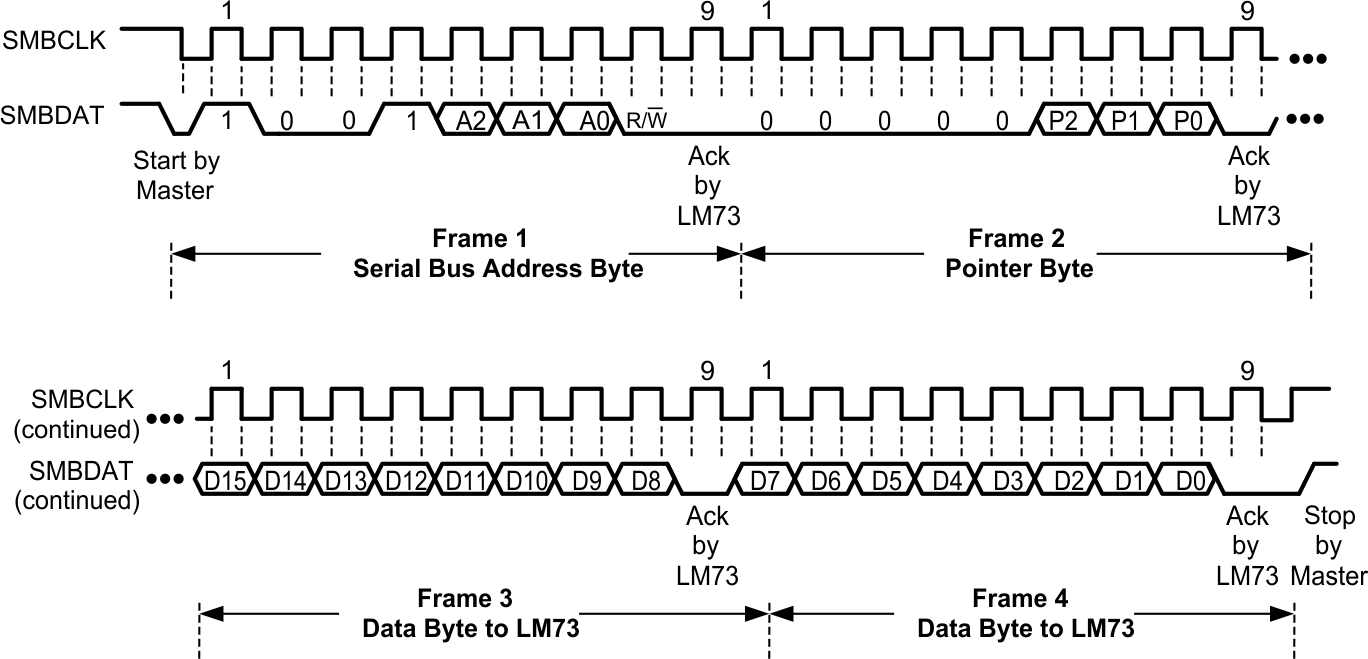 Figure 12. Typical 2-Byte Write
7.4 Device Functional Modes
7.4.1 Shutdown Mode
Shutdown Mode is enabled by writing a “1” to the Full Power Down Bit, Bit 7 of the Configuration Register, and holding it high for at least the specified maximum conversion time at the existing temperature resolution setting. (see Temperature Conversion Time specifications under the Temperature-to-Digital Converter Characteristics). For example, if the LM73-Q1 is set for 12-bit resolution before shutdown, then Bit 7 of the Configuration register must go high and stay high for the specified maximum conversion time for 12-bits resolution.
The LM73-Q1 will always finish a temperature conversion and update the temperature registers before shutting down.
Writing a “0” to the Full Power Down Bit restores the LM73-Q1 to normal mode. The user should wait at least the specified maximum conversion time, at the existing resolution setting, before accurate data appears in the temperature register.
7.5 Register Map
7.5.1 LM73-Q1 Registers
The LM73-Q1's internal registers are selected by the Pointer register. The Pointer register latches the last location that it was set to. The pointer register and all internal registers are described below. All registers reset at device power up.
7.5.1.1 Pointer Register
The diagram below shows the Pointer Register, the six internal registers to which it points, and their associated pointer addresses.
| P7 | P6 | P5 | P4 | P3 | P2 | P1 | P0 |
|---|---|---|---|---|---|---|---|
| 0 | 0 | 0 | 0 | 0 | Register Select | ||
| Bits | Name | Description |
|---|---|---|
| 7:3 | Not Used | Must write zeros only. |
| 2:0 | Register Select | Pointer address. Points to desired register. See table below. |
| P2 | P1 | P0 | REGISTER(1) |
|---|---|---|---|
| 0 | 0 | 0 | Temperature |
| 0 | 0 | 1 | Configuration |
| 0 | 1 | 0 | THIGH |
| 0 | 1 | 1 | TLOW |
| 1 | 0 | 0 | Control / Status |
| 1 | 1 | 1 | Identification |
(a) the LM73-Q1 will not acknowledge the address and
(b) the Pointer Register will continue to contain the last value stored in it.
7.5.1.2 Temperature Data Register
Pointer Address 00h (Read Only)
Reset State: 7FFCh (+255.96875°C)
One-Shot State: 8000h (-256°C)
| D15 | D14 | D13 | D12 | D11 | D10 | D9 | D8 |
|---|---|---|---|---|---|---|---|
| SIGN | 128°C | 64°C | 32°C | 16°C | 8°C | 4°C | 2°C |
| D7 | D6 | D5 | D4 | D3 | D2 | D1 | D0 |
|---|---|---|---|---|---|---|---|
| 1°C | 0.5°C | 0.25°C | 0.125°C | 0.0625°C | 0.03125°C | reserved | reserved |
| Bits | Name | Description |
|---|---|---|
| 15:2 | Temperature Data | Represents the temperature that was measured by the most recent temperature conversion. On Power-up, this data is invalid until the Data Available (DAV) bit in the Control/Status register is high (after the completion of the first temperature conversion). The resolution is user-programable from 11-bit resolution (0.25°C/LSB) through 14-bit resolution (0.03125°C/LSB). The desired resolution is programmed with bits 5 and 6 of the Control/Status register. |
| 1:0 | Not Used | Return zeros upon read. |
7.5.1.3 Configuration Register
Pointer Address 01h (R/W)
Reset State: 40h
| D7 | D6 | D5 | D4 | D3 | D2 | D1 | D0 |
|---|---|---|---|---|---|---|---|
| PD | reserved | ALRT EN | ALRT POL | ALRT RST | ONE SHOT | reserved | |
| Bits | Name | Description |
|---|---|---|
| 7 | Full Power Down | Writing a 1 to this bit and holding it high for at least the specified maximum conversion time, at the existing temperature resolution setting, puts the LM73-Q1 in shutdown mode for power conservation. Writing a 0 to this bit restores the LM73-Q1 to normal mode. Waiting one specified maximum conversion time for the existing resolution setting assures accurate data in the temperature register. |
| 6 | reserved | User must write only a 1 to this bit |
| 5 | ALERT Enable | A 0 in this location enables the ALERT output. A 1 disables it. This bit also controls the ALERT Status bit (the Control/Status Register, Bit 3) since that bit reflects the state of the Alert pin. |
| 4 | ALERT Polarity | When set to 1, the ALERT pin and ALERT Status bit are active-high. When 0, it is active-low. |
| 3 | ALERT Reset | Writing a 1 to this bit resets the ALERT pin and the ALERT Status bit. It will always be 0 when read. |
| 2 | One Shot | When in shutdown mode (Bit 7 is 1), initiates a single temperature conversion and update of the temperature register with new temperature data. Has no effect when in continuous conversion mode (i.e., when Bit 7 is 0). Always returns a 0 when read. |
| 1:0 | Reserved | User must write only a 0 to these bits. |
7.5.1.4 THIGH Upper-Limit Register
Pointer Address 02h (R/W)
Reset State: 7FE0h (+255.75°C)
| D15 | D14 | D13 | D12 | D11 | D10 | D9 | D8 |
|---|---|---|---|---|---|---|---|
| SIGN | 128°C | 64°C | 32°C | 16°C | 8°C | 4°C | 2°C |
| D7 | D6 | D5 | D4 | D3 | D2 | D1 | D0 |
|---|---|---|---|---|---|---|---|
| 1°C | 0.5°C | 0.25°C | reserved | ||||
| Bits | Name | Description |
|---|---|---|
| 15:5 | Upper-Limit Temperature | If the measured temperature that is stored in this register exceeds this user-programmable upper temperature limit, the ALERT pin will go active and the THIGH flag in the Control/Status register will be set to 1. Two's complement format. |
| 4:0 | Reserved | Returns zeros upon read. Recommend writing zeros only in these bits. |
7.5.1.5 TLOW Lower-Limit Register
Pointer Address 03h (R/W)
Reset State: 8000h (–256°C)
| D15 | D14 | D13 | D12 | D11 | D10 | D9 | D8 |
|---|---|---|---|---|---|---|---|
| SIGN | 128°C | 64°C | 32°C | 16°C | 8°C | 4°C | 2°C |
| D7 | D6 | D5 | D4 | D3 | D2 | D1 | D0 |
|---|---|---|---|---|---|---|---|
| 1°C | 0.5°C | 0.25°C | reserved | ||||
| Bits | Name | Description |
|---|---|---|
| 15:5 | Lower-Limit Temperature | If the measured temperature that is stored in the temperature register falls below this user-programmable lower temperature limit, the ALERT pin will be deactivated and the TLOW flag in the Control/Status register will be set to 1. Two's complement format. |
| 4:0 | Reserved | Returns zeros upon read. Recommend writing zeros only in these bits. |
7.5.1.6 Control/Status Register
Pointer Address 04h (R/W)
Reset State: 08h
| D7 | D6 | D5 | D4 | D3 | D2 | D1 | D0 |
|---|---|---|---|---|---|---|---|
| TO_DIS | RES1 | RES0 | reserved | ALRT_STAT | THI | TLOW | DAV |
| BITS | NAME | DESCRIPTION |
|---|---|---|
| 7 | Time-Out Disable | Disable the time-out feature on the SMBDAT and SMBCLK lines if set to 1. Setting this bit turns off the bus-idle timers, enabling the LM73-Q1 to operate at lowest shutdown current. |
| 6:5 | Temperature Resolution | Selects one of four user-programmable temperature data resolutions 00: 0.25°C/LSB, 11-bit word (10 bits plus Sign) 01: 0.125°C/LSB, 12-bit word (11 bits plus Sign) 10: 0.0625°C/LSB, 13-bit word (12 bits plus Sign) 11: 0.03125°C/LSB, 14-bit word (13 bits plus Sign) |
| 4 | reserved | Always returns zero when read. Recommend customer write zero only. |
| 3 | ALERT Pin Status | Value is 0 when ALERT output pin is low. Value is 1 when ALERT output pin is high. The ALERT output pin is reset under any of the following conditions: (1) Cleared by writing a 1 to the ALERT Reset bit in the configuration register, (2) Measured temperature falls below the TLOW limit, or (3) cleared via the ARA sequence. Recommend customer write zero only. |
| 2 | Temperature High Flag | Bit is set to 1 when the measured temperature exceeds the THIGH limit stored in the programmable THIGH register. Flag is reset to 0 when both of the following conditions are met: (1) measured temperature no longer exceeds the programmed THIGH limit and (2) upon reading the Control/Status register. If the temperature is not longer above the THIGH limit, this status bit remains set until it is read by the master so that the system can check the history of what caused the ALERT output to go active. This bit is not cleared after every read if the measured temperature is still above the THIGH limit. |
| 1 | Temperature Low Flag | Bit is set to 1 when the measured temperature falls below the TLOW limit stored in the programmable TLOW register. Flag is reset to 0 when both of the following conditions are met: (1) measured temperature is no longer below the programmed TLOW limit and (2) upon reading the Control/Status register. If the temperature is no longer below the TLOW limit, the status bit remains set until it is read by the master so that the system can check the history of what cause the ALERT output to go active. This bit is not cleared after every read if temperature is still below TLOW limit. |
| 0 | Data Available Flag | This bit is 0 when the LM73-Q1 is in the process of converting a new temperature. It is 1 when the conversion is done. After initiating a temperature conversion while operating in the one-shot mode, this status bit can be monitored to indicate when the conversion is done. After triggering the one-shot conversion, the data in the temperature register is invalid until this bit is high (that is, after completion of the conversion). On power-up, the LM73-Q1 is in continuous conversion mode; while in continuous conversion mode (the default mode after power-on reset) this bit will always be high. Recommend customer write zero only. |
7.5.1.7 Identification Register
Pointer Address 07h (Read Only)
Reset State: 0190h
| D15 | D14 | D13 | D12 | D11 | D10 | D9 | D8 |
|---|---|---|---|---|---|---|---|
| 0 | 0 | 0 | 0 | 0 | 0 | 0 | 1 |
| D7 | D6 | D5 | D4 | D3 | D2 | D1 | D0 |
|---|---|---|---|---|---|---|---|
| 1 | 0 | 0 | 1 | 0 | 0 | 0 | 0 |
| BITS | NAME | DESCRIPTION |
|---|---|---|
| 15:8 | Manufacturer Identification Byte | Always returns 01h to uniquely identify the manufacturer as Texas Instruments. |
| 7:4 | Product Identification Nibble | Always returns 9h to uniquely identify this part as the LM73-Q1 Temperature Sensor. |
| 3:0 | Die Revision Step Nibble | Always returns 0h to uniquely identify the revision as level zero. |