ZHCSLY9A October 2020 – December 2020 LM7310
PRODUCTION DATA
- 1 特性
- 2 应用
- 3 说明
- 4 Revision History
- 5 Pin Configuration and Functions
- 6 Specifications
-
7 Detailed Description
- 7.1 Overview
- 7.2 Functional Block Diagram
- 7.3
Feature Description
- 7.3.1 Input Reverse Polarity Protection
- 7.3.2 Undervoltage Protection (UVLO & UVP)
- 7.3.3 Overvoltage Lockout (OVLO)
- 7.3.4 Inrush Current control and Fast-trip
- 7.3.5 Analog Load Current Monitor Output
- 7.3.6 Reverse Current Protection
- 7.3.7 Overtemperature Protection (OTP)
- 7.3.8 Fault Response
- 7.3.9 Power Good Indication (PG)
- 7.4 Device Functional Modes
- 8 Application and Implementation
- 9 Power Supply Recommendations
- 10Layout
- 11Device and Documentation Support
- 12Mechanical, Packaging, and Orderable Information
7.3.9 Power Good Indication (PG)
The LM73100 provides an active high digital output (PG) which serves as a power good indication signal and is asserted high depending on the voltage at the PGTH pin along with the device state information. The PG is an open-drain pin and needs to be pulled up to an external supply.
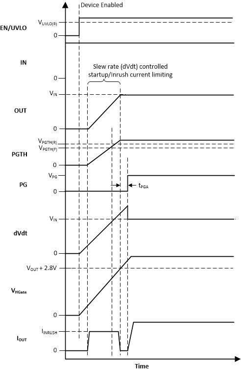
After power up, PG is pulled low initially. The device initiates a inrush sequence in which the HFET is turned on in a controlled manner. When the HFET gate voltage reaches the full overdrive indicating that the inrush sequence is complete and the voltage at PGTH is above VPGTH(R), the PG is asserted after a de-glitch time (tPGA).
PG is de-asserted if at any time during normal operation, the voltage at PGTH falls below VPGTH(F), or the device detects a fault. The PG de-assertion de-glitch time is tPGD.
 Figure 7-10 LM73100 PG Timing Diagram
|
Event |
Protection Response |
PG Pin |
PG Delay |
|---|---|---|---|
|
Undervoltage (UVP or UVLO) |
Shutdown |
L |
|
|
Input Reverse Polarity |
Shutdown |
L |
|
|
Overvoltage (OVLO) |
Shutdown |
L |
tPGD |
|
Steady State |
N/A |
H (If PGTH pin voltage > VPGTH(R)) L (If PGTH pin voltage < VPGTH(F)) |
tPGA tPGD |
|
Transient overcurrent during steady state |
Fast-trip |
H (If PGTH pin voltage > VPGTH(R)) L (If PGTH pin voltage < VPGTH(F)) |
tPGA tPGD |
|
Reverse current ((VOUT - VIN) > VREVTH) |
Reverse current blocking |
L |
tPGD |
|
Overtemperature |
Shutdown |
L |
tPGD |
When there is no supply to the device, the PG pin is expected to stay low. However, there is no active pull-down in this condition to drive this pin all the way down to 0 V. If the PG pin is pulled up to an independent supply which is present even if the device is unpowered, there can be a small voltage seen on this pin depending on the pin sink current, which is a function of the pull-up supply voltage and resistor. Minimize the sink current to keep this pin voltage low enough not to be detected as a logic HIGH by associated external circuits in this condition.