ZHCSNL2A February   2022  – May 2022 LM74502-Q1 , LM74502H-Q1

PRODUCTION DATA  

  1. 特性
  2. 应用
  3. 说明
  4. Revision History
  5. Device Comparison Table
  6. Pin Configuration and Functions
  7. Specifications
    1. 7.1 Absolute Maximum Ratings
    2. 7.2 ESD Ratings
    3. 7.3 Recommended Operating Conditions
    4. 7.4 Thermal Information
    5. 7.5 Electrical Characteristics
    6. 7.6 Switching Characteristics
    7. 7.7 Typical Characteristics
  8. Parameter Measurement Information
  9. Detailed Description
    1. 9.1 Overview
    2. 9.2 Functional Block Diagram
    3. 9.3 Feature Description
      1. 9.3.1 Input Voltage (VS)
      2. 9.3.2 Charge Pump (VCAP)
      3. 9.3.3 Gate Driver (GATE an SRC)
        1. 9.3.3.1 Inrush Current Control
      4. 9.3.4 Enable and Undervoltage Lockout (EN/UVLO)
      5. 9.3.5 Overvoltage Protection (OV)
    4. 9.4 Device Functional Modes
      1. 9.4.1 Shutdown Mode
      2. 9.4.2 Conduction Mode
  10. 10Application and Implementation
    1. 10.1 Application Information
    2. 10.2 Typical Application
      1. 10.2.1 Design Requirements
      2. 10.2.2 Detailed Design Procedure
        1. 10.2.2.1 Design Considerations
        2. 10.2.2.2 MOSFET Selection
        3. 10.2.2.3 Overvoltage Protection
        4. 10.2.2.4 Charge Pump VCAP, Input and Output Capacitance
      3. 10.2.3 Selection of TVS Diodes for 12-V Battery Protection Applications
      4. 10.2.4 Selection of TVS Diodes and MOSFET for 24-V Battery Protection Applications
      5. 10.2.5 Application Curves
    3. 10.3 Surge Stopper Using LM74502-Q1, LM74502H-Q1
      1. 10.3.1 VS Capacitance, Resistor R1 and Zener Clamp (DZ)
      2. 10.3.2 Overvoltage Protection
      3. 10.3.3 MOSFET Selection
    4. 10.4 Fast Turn-On and Turn-Off High Side Switch Driver Using LM74502H-Q1
  11. 11Power Supply Recommendations
  12. 12Layout
    1. 12.1 Layout Guidelines
    2. 12.2 Layout Example
  13. 13Device and Documentation Support
    1. 13.1 接收文档更新通知
    2. 13.2 支持资源
    3. 13.3 Trademarks
    4. 13.4 Electrostatic Discharge Caution
    5. 13.5 术语表
  14. 14Mechanical, Packaging, and Orderable Information

封装选项

请参考 PDF 数据表获取器件具体的封装图。

机械数据 (封装 | 引脚)
  • DDF|8
散热焊盘机械数据 (封装 | 引脚)
订购信息

Application Curves

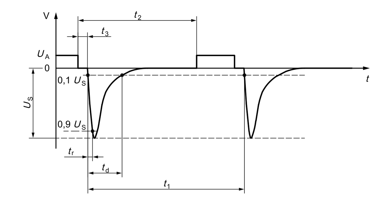
GUID-5EC1293C-8335-46EC-BE94-35DEC5369859-low.pngFigure 10-3 ISO 7637-2 Pulse 1
GUID-20220406-SS0I-NJKC-0PHC-GQ0JBPGHG8JW-low.png
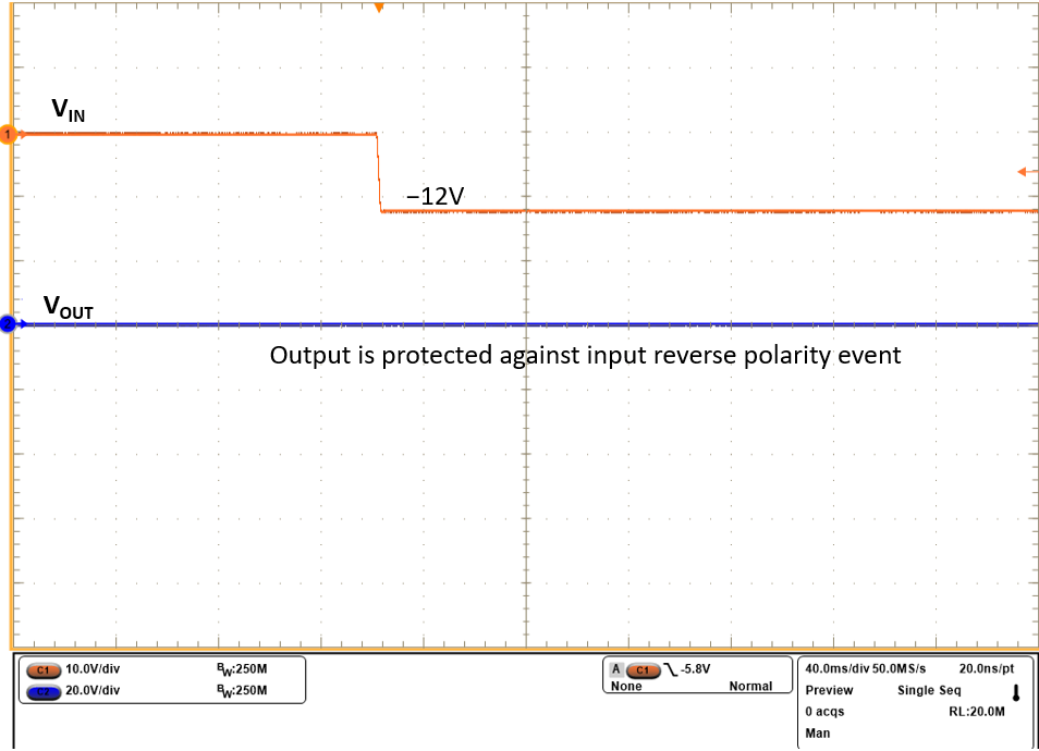
Time (40 ms/DIV)
Figure 10-5 Start-up with Input Reverse Voltage (–12 V)
GUID-20220406-SS0I-C3TT-G651-0RHXXKGXHCKZ-low.png
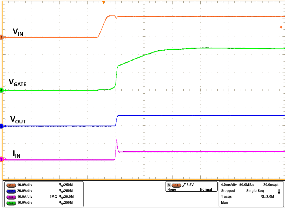
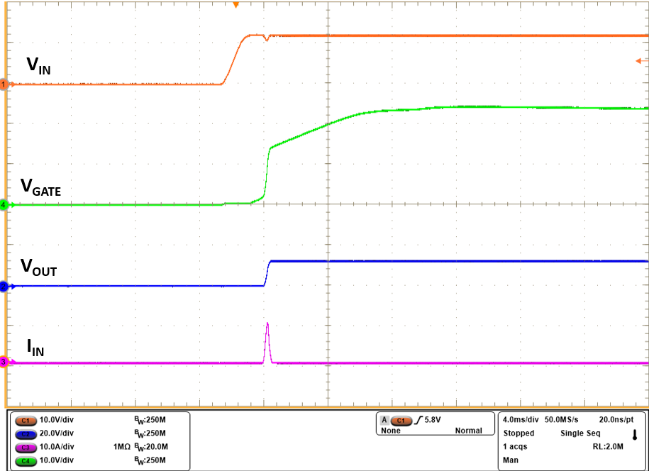
Time (4 ms/DIV)
Figure 10-7 Start-up with 5-A Load
GUID-20220406-SS0I-RXG8-4BLM-HWMQTJGJSL6K-low.png
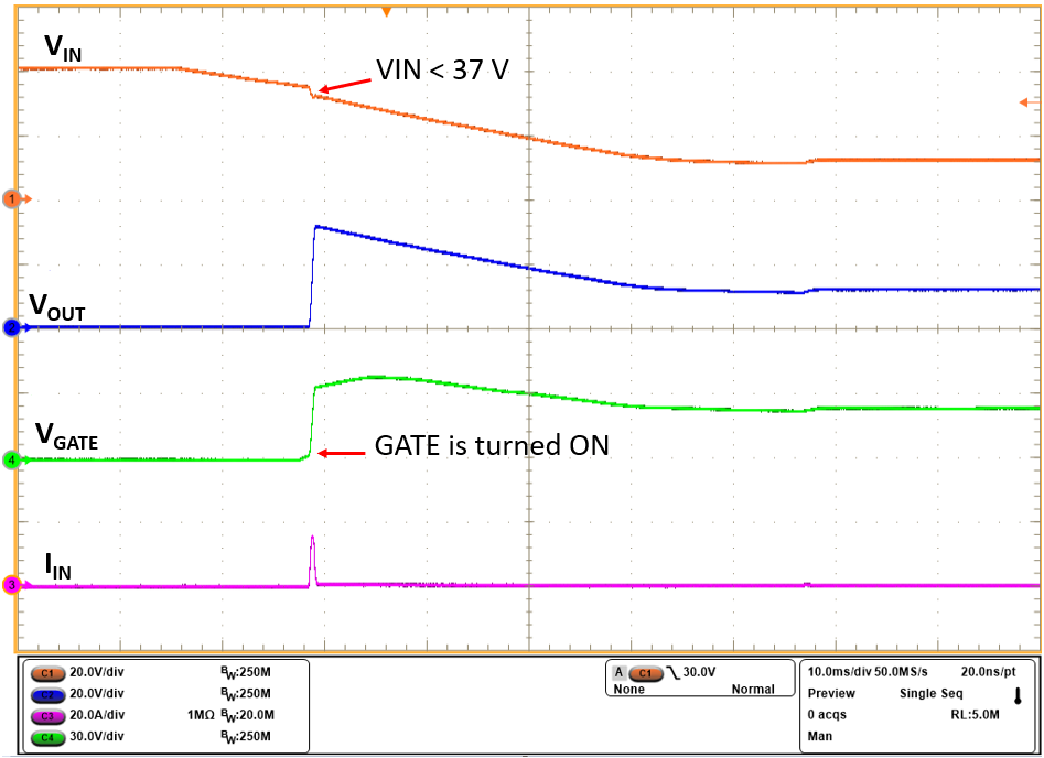
Time (10 ms/DIV)
Figure 10-9 Overvoltage Recovery
GUID-20220406-SS0I-NWJC-BBPZ-DTLNBPCPB4K2-low.png
Time (2.5 ms/DIV)
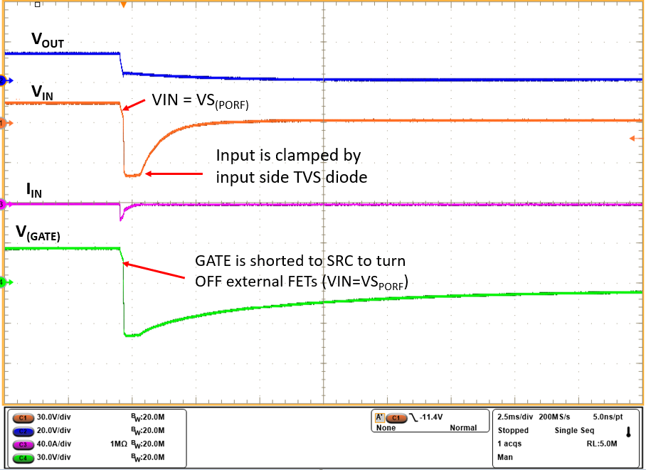
Figure 10-4 Response to ISO 7637-2 Pulse 1 (–150 V)
GUID-20220406-SS0I-MZZK-5PGQ-PBC54CFD3CXP-low.png
Time (4 ms/DIV)
Figure 10-6 Start-up with No Load
GUID-20220406-SS0I-QRZK-BMNP-XKX1TN12SDML-low.png
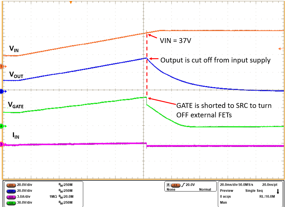
Time (20 ms/DIV)
Figure 10-8 Overvoltage Cutoff Response (37 V)
GUID-20220406-SS0I-XZR7-VGMD-WTB05SWFGSK1-low.png
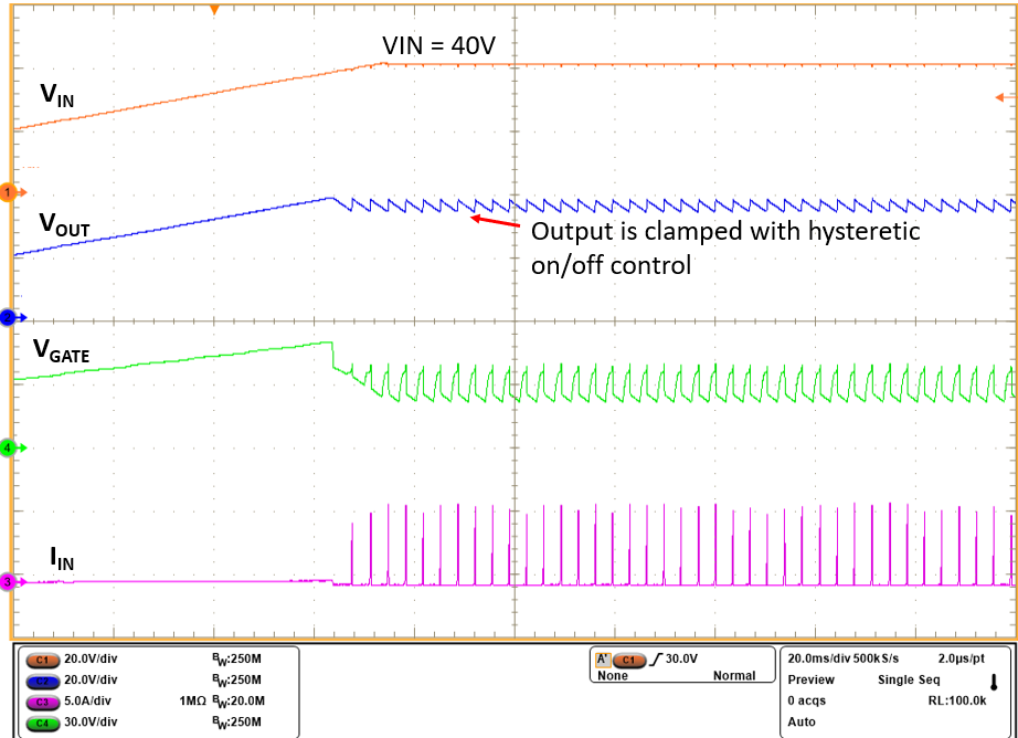
Time (20 ms/DIV)
Figure 10-10 Overvoltage Clamp Response