ZHCSE83A July 2015 – October 2015 LM74610-Q1
PRODUCTION DATA.
- 1 特性
- 2 应用
- 3 说明
- 4 修订历史记录
- 5 Pin Configuration and Functions
- 6 Specifications
- 7 Detailed Description
- 8 Application and Implementation
- 9 Power Supply Recommendations
- 10Layout
- 11器件和文档支持
- 12机械封装和可订购信息
6 Specifications
6.1 Absolute Maximum Ratings
over operating free-air temperature range (unless otherwise noted) (1)| MIN | MAX | UNIT | |
|---|---|---|---|
| Cathode to Anode (For a 2ms time duration) (2), (3) | -3 | 45 | V |
| Cathode to Anode (Continuous)(3) | -3 | 42 | V |
| VcapH to VcapL | -0.3 | 7 | V |
| Anode to VcapL | -0.3 | 3 | V |
| Gate Drive, Gate Pull Down to VcapL | -0.3 | 7 | V |
| Ambient Temperature (TA-MAX) (4) | -40 | 125 | °C |
| Case Temperature (TC-MAX) | -40 | 125 | °C |
| Storage temperature range, Tstg | -65 | 150 | °C |
(1) Stresses beyond those listed under Absolute Maximum Ratings may cause permanent damage to the device. These are stress ratings only, which do not imply functional operation of the device at these or any other conditions beyond those indicated under Recommended Operating Conditions. Exposure to absolute-maximum-rated conditions for extended periods may affect device reliability.
(2) 42V continuous (and 45V transients for 2ms) absmax condition from Cathode to Anode. Suitable to use with TVS SMBJ28A and SMBJ14A at the anode.
(3) Reverse voltage rating only. There is no positive voltage limitation for the LM74610-Q1 Anode terminal.
(4) The device performance is ensured over this Ambient Temperature range as long the Case Temperature does not exceed the MAX value.
6.2 ESD Ratings
| VALUE | UNIT | |||
|---|---|---|---|---|
| V(ESD) | Electrostatic discharge(1) | Human body model (HBM), per AEC Q100-002(2) | ±4000 | V |
| Charged-device model (CDM), per AEC Q100-011 | ±750 | |||
(1) AEC Q100-002 indicates that HBM stressing shall be in accordance with the ANSI/ESDA/JEDEC JS-001 specification.
(2) The human body model is a 100 pF capacitor discharged through a 1.5 kΩ resistor into each pin.
6.3 Recommended Operating Conditions
over operating free-air temperature range (unless otherwise noted)| MIN | NOM | MAX | UNIT | ||
|---|---|---|---|---|---|
| Cathode To Anode | 42 | V | |||
| Ambient Temperature (TA-MAX) | -40 | 125 | °C | ||
| Case Temperature (TC-MAX) | 125 | °C | |||
6.4 Thermal Information
| THERMAL METRIC(1) | LM74610-Q1 VSSOP 8 PINS | UNIT | |
|---|---|---|---|
| RθJA | Junction-to-ambient thermal resistance | 181 | °C/W |
| RθJC(top) | Junction-to-case (top) thermal resistance | 73 | |
| RθJB | Junction-to-board thermal resistance | 102 | |
| ψJT | Junction-to-top characterization parameter | 11 | |
| ψJB | Junction-to-board characterization parameter | 100 | |
(1) For more information about traditional and new thermal metrics, see the IC Package Thermal Metrics application report, SPRA953.
6.5 Electrical Characteristics
TA= 25°C unless otherwise noted. Minimum and Maximum limits are specified through test, design, validation or statistical correlation. Typical values represent the most likely parametric norm at TA= 25°C and are provided for reference purpose only. VAnode-Cathode= 0.55V for all tests.(1)| PARAMETER | TEST CONDITIONS | MIN | TYP | MAX | UNIT | |
|---|---|---|---|---|---|---|
| VAnode to Cathode | Minimum Startup Voltage across External MOSFET's Body Diode | External MOSFET VGS = 0V | 0.48 | V | ||
| Vcap Threshold | Charge Pump Capacitor Drive Thresholds | Vcap Upper Threshold | 6.3 | V | ||
| Vcap Lower Threshold | 5.15 | V | ||||
| IGate up | Gate Drive Pull up current | VGate to Anode = 2V | 8.9 | 9.4 | µA | |
| IGate down | Gate Drive pull down current during forward voltage | VGate to Anode = 4V | 6.35 | 6.8 | µA | |
| IGate pull down | Gate drive pull down current when reverse voltage is sensed | VGate Pull Down = VAnode + 2V | 160 | mA | ||
| ICharge Current | Charging current for the charge pump capacitor | VAnode to Cathode = 0.55 V | 40 | 46 | µA | |
| IDischarge Current | VCAP Current Consumption to power the controller when MOSFET is ON | Vcap = 6.6V | 0.95 | µA | ||
| TRecovery | Time to shut off MOSFET when voltage is reversed (Equivalent to diode reverse recovery time) | VAnode to Cathode = -20 mV Cgate = 4 nF |
2.2 | 5(2) | µs | |
| D | Duty Cycle | Iload = 3 A, TA = 25°C | 98% | |||
| Iload = 3 A, TA = 125°C | 92% | |||||
| ILKG | Reverse Leakage Current | VAnode to Cathode = -13.5 V | 60 | 110(2) | µA | |
| Iq | Quiescent Current to GND | 0 | µA | |||
| IAnode | Current into Anode pin | Current into Anode pin when VAnode - Cathode = 0.3V. | 30 | µA |
(1) Absolute Maximum Ratings are limits beyond which damage to the device may occur. Operating Ratings are conditions under which operation of the device is guaranteed. Operating Ratings do not imply guaranteed performance limits. For guaranteed performance limits and associated test conditions, see the table of Electrical Characteristics.
(2) Limit applies over the full Operating Temperature Range TA = -40°C to +125°C.
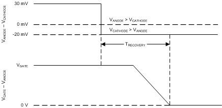 Figure 1. Gate Shut Down Timing in the Event of Reverse Polarity
6.6 Typical Characteristics
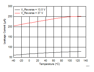 Figure 2. Reverse Leakage at Negative Voltages
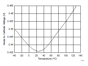 Figure 3. Anode to Cathode Startup Voltage
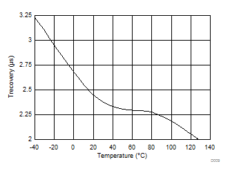 Figure 4. Reverse Recovery Time (TRecovery)
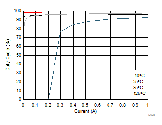 Figure 6. Duty Cycle of the Output Voltage at Startup
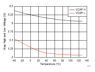 Figure 5. VcapH and VcapL Voltage Threshold
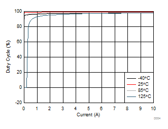 Figure 7. Duty Cycle of the Output Voltage