ZHCSMT1 September 2021 LM74700-EP
PRODUCTION DATA
- 1 特性
- 2 应用
- 3 说明
- 4 Revision History
- 5 Pin Configuration and Functions
- 6 Specifications
- 7 Parameter Measurement Information
- 8 Detailed Description
-
9 Application and Implementation
- 9.1 Application Information
- 9.2 Typical Application
- 9.3 OR-ing Application Configuration
- 10Power Supply Recommendations
- 11Layout
- 12Device and Documentation Support
- 13Mechanical, Packaging, and Orderable Information
6.7 Typical Characteristics
Figure 6-1 Shutdown Supply Current vs Supply Voltage
Figure 6-3 Enable Sink Current vs Supply Voltage
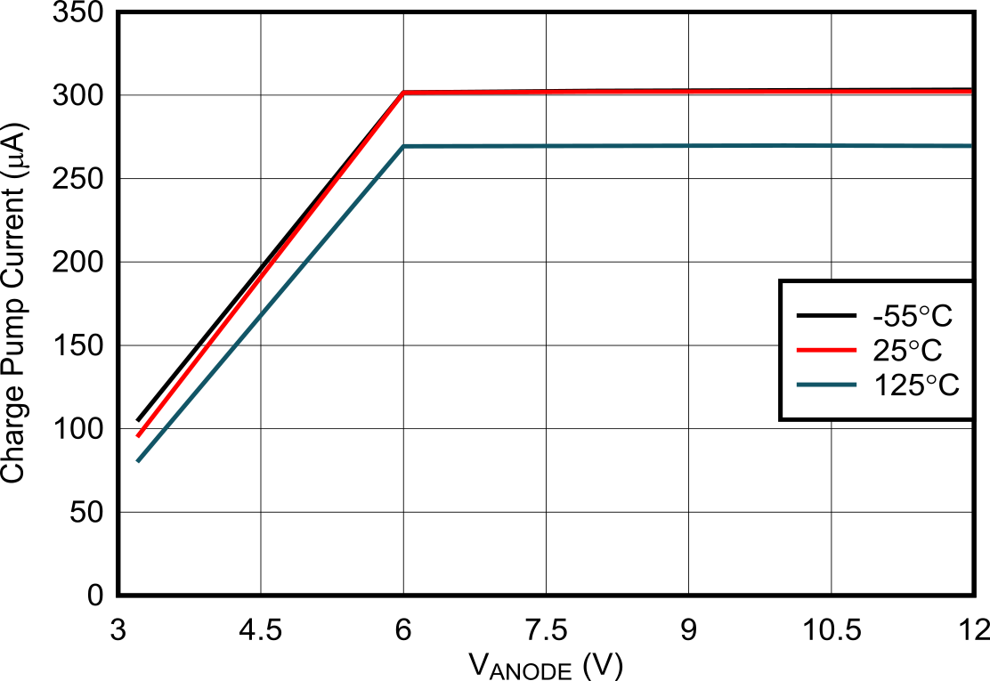 Figure 6-5 Charge Pump Current vs Supply Voltage at VCAP = 6 V
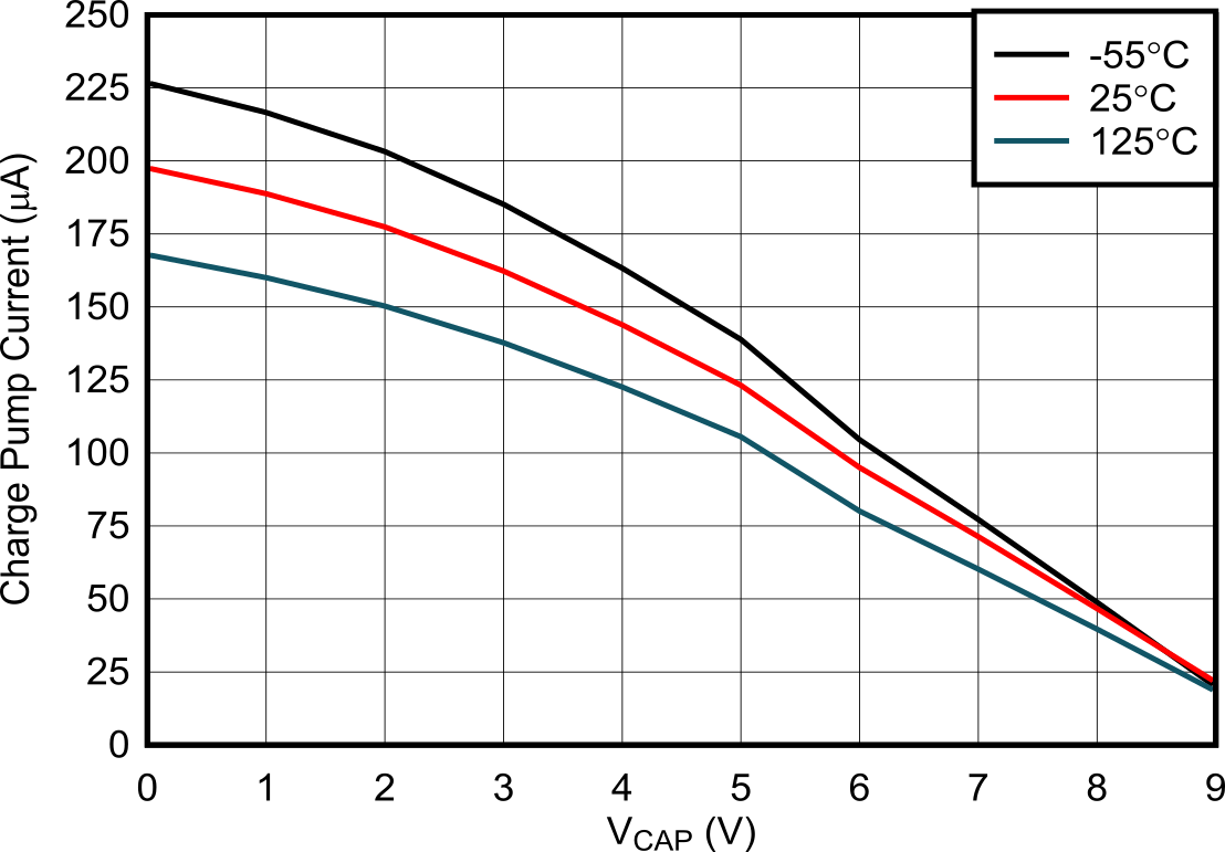 Figure 6-7 Charge Pump V-I Characteristics at VANODE = 3.2 V
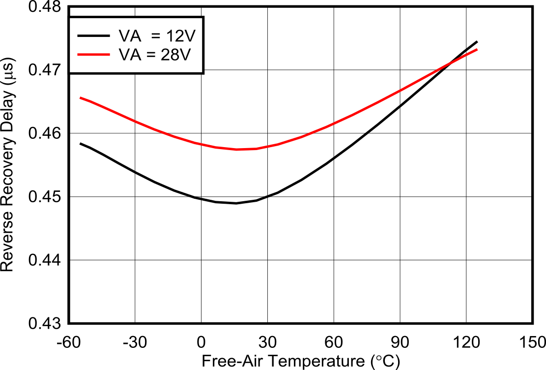 Figure 6-9 Reverse Current Blocking Delay vs Temperature
 Figure 6-11 Enable to Gate Delay vs Temperature
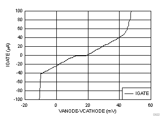 Figure 6-13 Gate Current vs Forward Voltage Drop.
 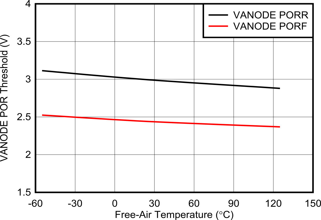 Figure 6-15 VANODE POR Threshold vs Temperature.
 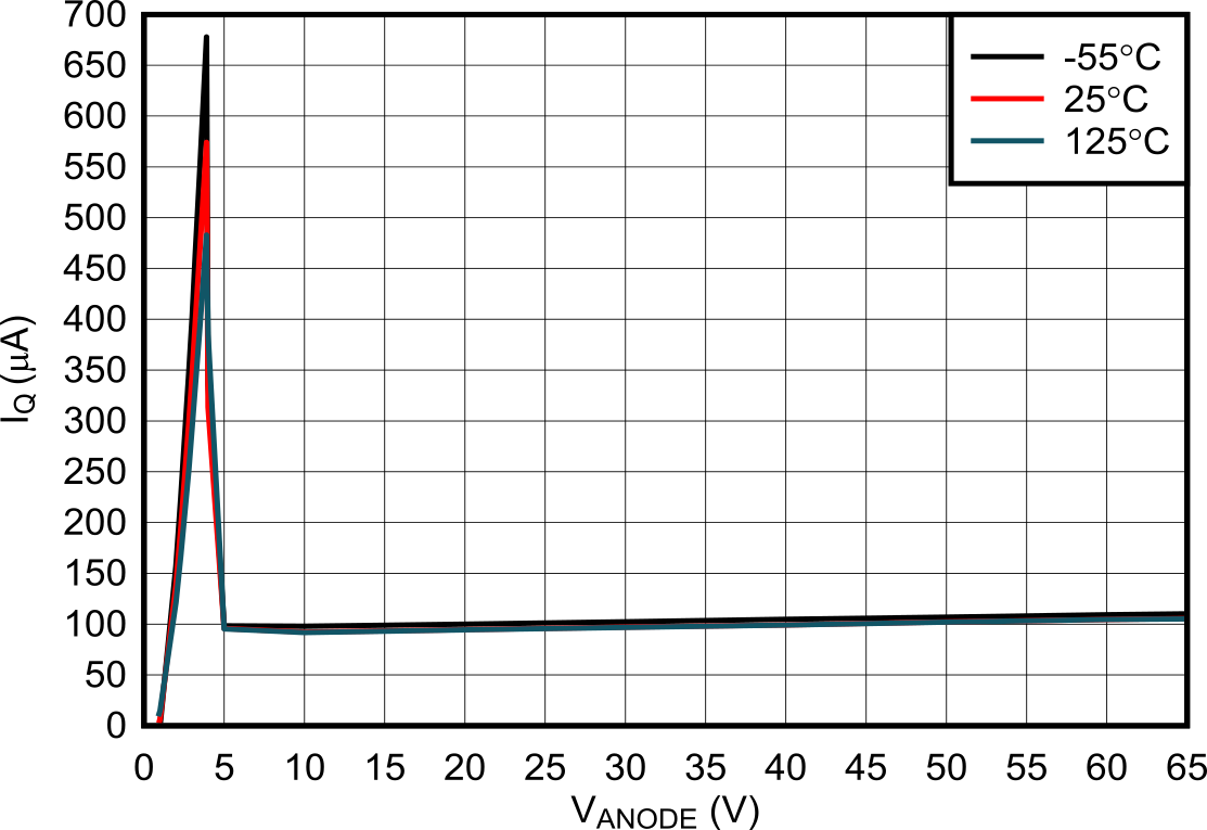 Figure 6-2 Operating Quiescent Current vs Supply Voltage.
 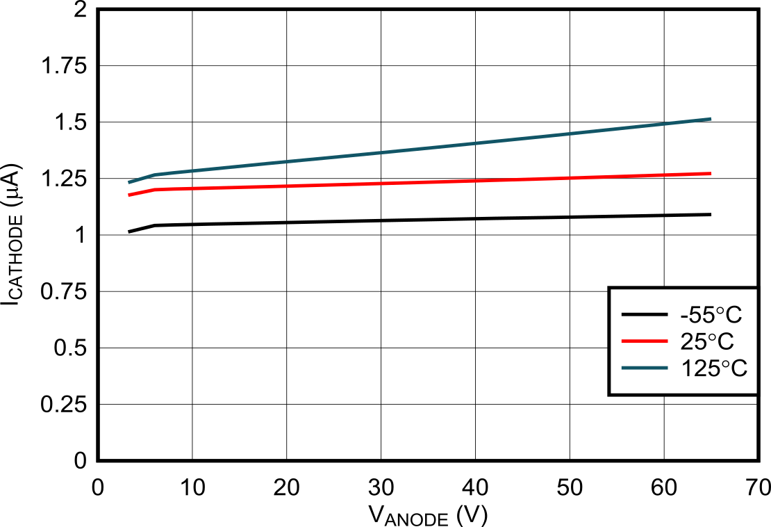 Figure 6-4 Cathode Sink Current vs Supply Voltage
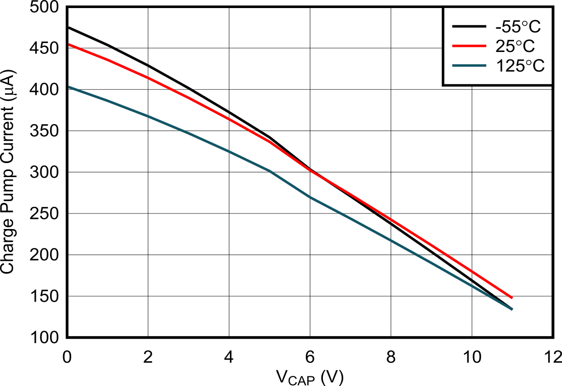 Figure 6-6 Charge Pump V-I Characteristics at VANODE > = 12 V
 Figure 6-8 Enable Falling Threshold vs Temperature
Figure 6-10 Forward Recovery Delay vs Temperature
Figure 6-12 Charge Pump ON/OFF Threshold vs Temperature
Figure 6-14 Charge Pump UVLO Threshold vs Temperature