ZHCSOW4B September 2021 – March 2022 LM74720-Q1
PRODUCTION DATA
- 1 特性
- 2 应用
- 3 说明
- 4 Revision History
- 5 Pin Configuration and Functions
- 6 Specifications
- 7 Parameter Measurement Information
- 8 Detailed Description
-
9 Application and Implementation
- 9.1 Application Information
- 9.2
Typical 12-V Reverse Battery Protection Application
- 9.2.1 Design Requirements for 12-V Battery Protection
- 9.2.2 Automotive Reverse Battery Protection
- 9.2.3
Detailed Design Procedure
- 9.2.3.1 Design Considerations
- 9.2.3.2 Boost Converter Components (C2, C3, L1)
- 9.2.3.3 Input and Output Capacitance
- 9.2.3.4 Hold-Up Capacitance
- 9.2.3.5 Overvoltage Protection and Battery Monitor
- 9.2.3.6 MOSFET Selection: Blocking MOSFET Q1
- 9.2.3.7 MOSFET Selection: Load Disconnect MOSFET Q2
- 9.2.3.8 TVS Selection
- 9.2.4 Application Curves
- 9.3 Do's and Don'ts
- 10Power Supply Recommendations
- 11Layout
- 12Device and Documentation Support
- 13Mechanical, Packaging, and Orderable Information
9.2.2.3 Input Micro-Short Protection: LV124 E-10
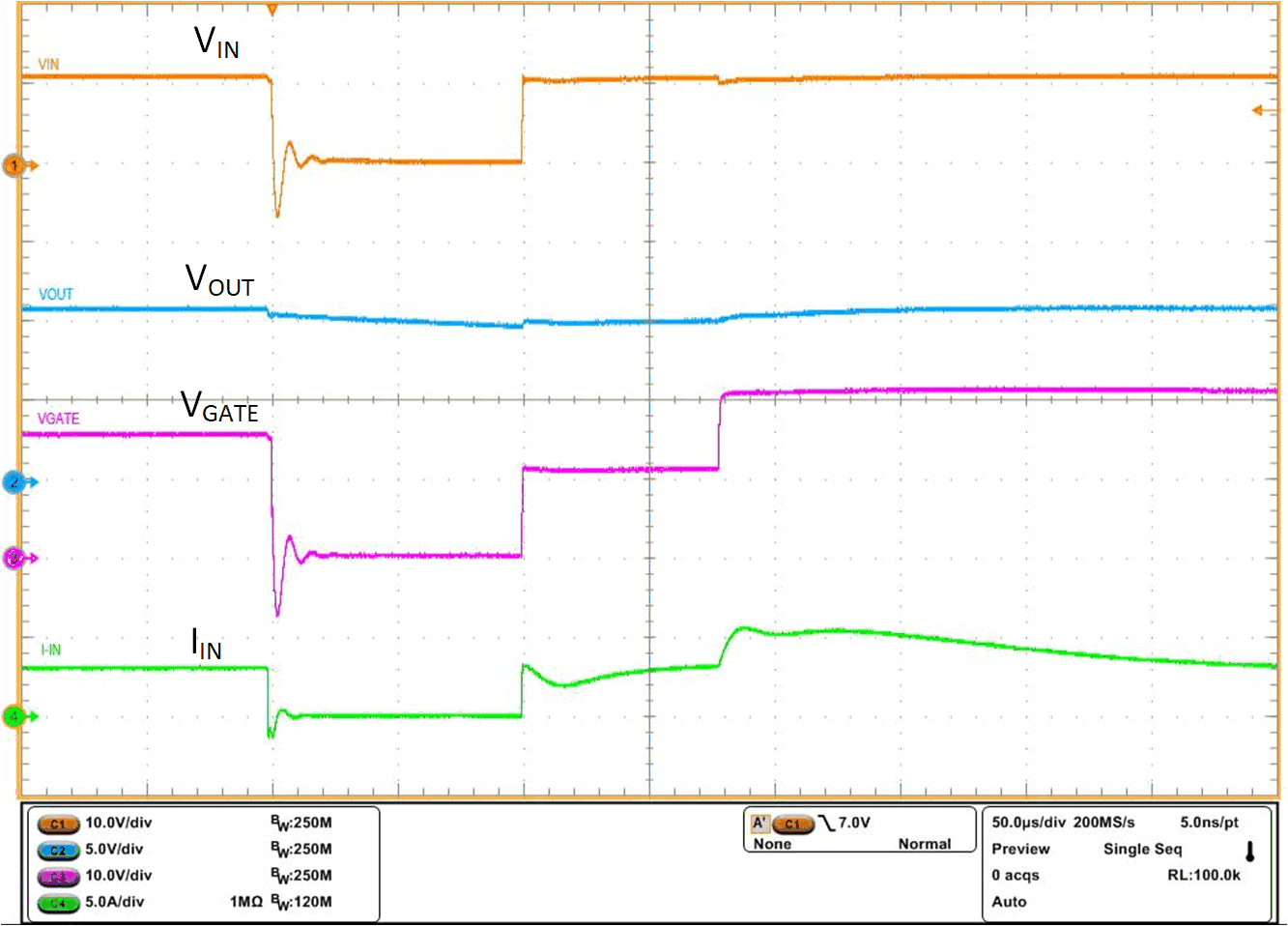
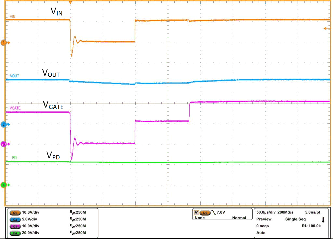
E-10 test specified in LV124 standard checks for immunity of electronic modules to short interruptions in power supply input due to contact issues or relay bounce. During this test (case 2), micro-short is applied on the input for a duration as low as 10 µs to several ms. For a functional pass status A, electronic modules are required to run uninterrupted during the E-10 test (case 2) with 100-µs duration. When input micro-short is applied for 100 µs, LM74720-Q1 quickly turns off MOSFET Q1 by shorting GATE to ANODE (source of MOSFET) within 0.5 µs to prevent the output from discharging and the PD remains ON keeping MOSFET Q2 ON, enabling fast recovery after the input short is removed.
Figure 9-5 shows performance of LM74720-Q1 during E10 input power supply interruption test case 2. After the input short is removed, input voltage recovers and MOSFET Q1 is turned back ON within 200 µs. Note that dual-gate drive topology allows MOSFET Q2 to remain ON during the test and helps in restoring the input power faster. Output voltage remains unperturbed during the entire duration, achieving functional status A.
 Figure 9-5 Input Micro-Short – LV124 E10 TC 2 100 µs
 Figure 9-6 Input Micro-Short – LV124 E10 TC 2 100 µs With PD