ZHCSOW4B September 2021 – March 2022 LM74720-Q1
PRODUCTION DATA
- 1 特性
- 2 应用
- 3 说明
- 4 Revision History
- 5 Pin Configuration and Functions
- 6 Specifications
- 7 Parameter Measurement Information
- 8 Detailed Description
-
9 Application and Implementation
- 9.1 Application Information
- 9.2
Typical 12-V Reverse Battery Protection Application
- 9.2.1 Design Requirements for 12-V Battery Protection
- 9.2.2 Automotive Reverse Battery Protection
- 9.2.3
Detailed Design Procedure
- 9.2.3.1 Design Considerations
- 9.2.3.2 Boost Converter Components (C2, C3, L1)
- 9.2.3.3 Input and Output Capacitance
- 9.2.3.4 Hold-Up Capacitance
- 9.2.3.5 Overvoltage Protection and Battery Monitor
- 9.2.3.6 MOSFET Selection: Blocking MOSFET Q1
- 9.2.3.7 MOSFET Selection: Load Disconnect MOSFET Q2
- 9.2.3.8 TVS Selection
- 9.2.4 Application Curves
- 9.3 Do's and Don'ts
- 10Power Supply Recommendations
- 11Layout
- 12Device and Documentation Support
- 13Mechanical, Packaging, and Orderable Information
9.2.4 Application Curves
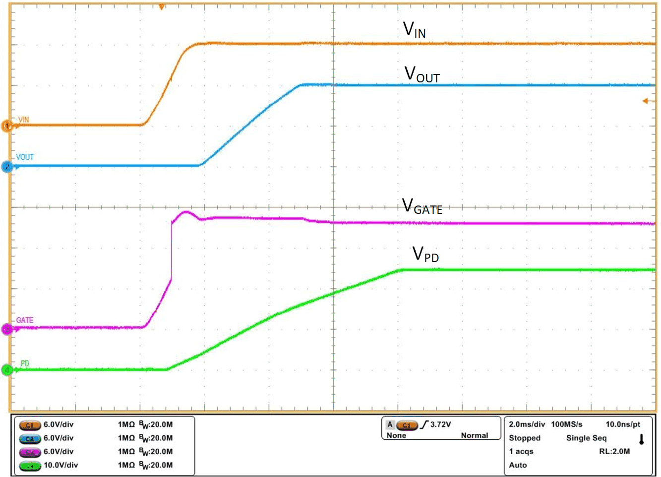 Figure 9-7 Start-up 12 V with EN
Pulled to VIN
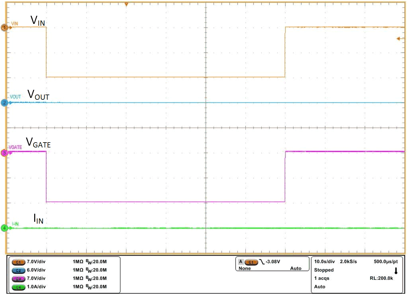 Figure 9-9 Reverse Input Voltage –14
V for 60 s
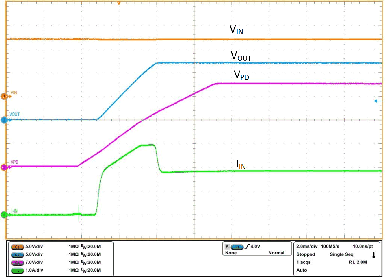 Figure 9-11 Inrush Current with 60-Ω
Load
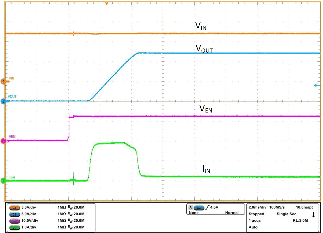 Figure 9-13 Output Turn-on with
Enable
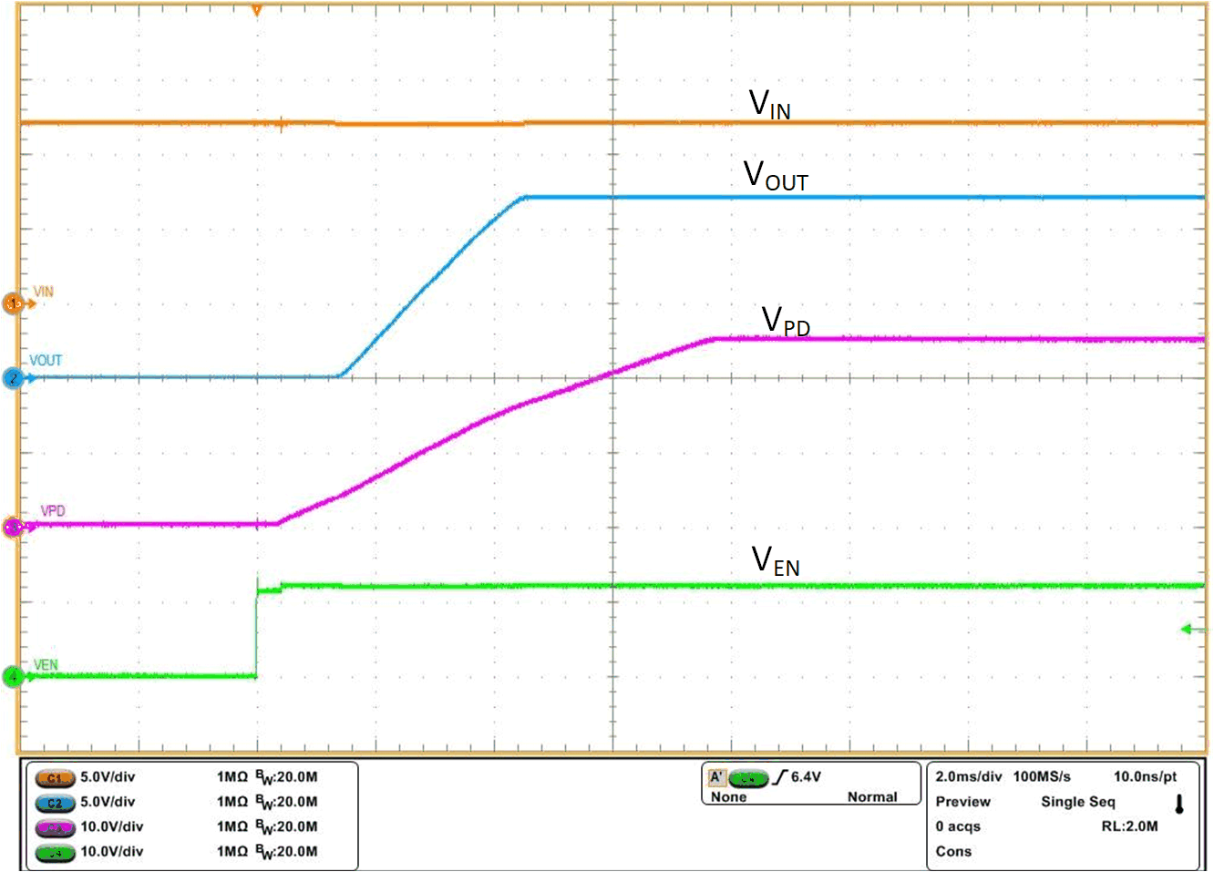 Figure 9-15 PD Turn-on with
Enable
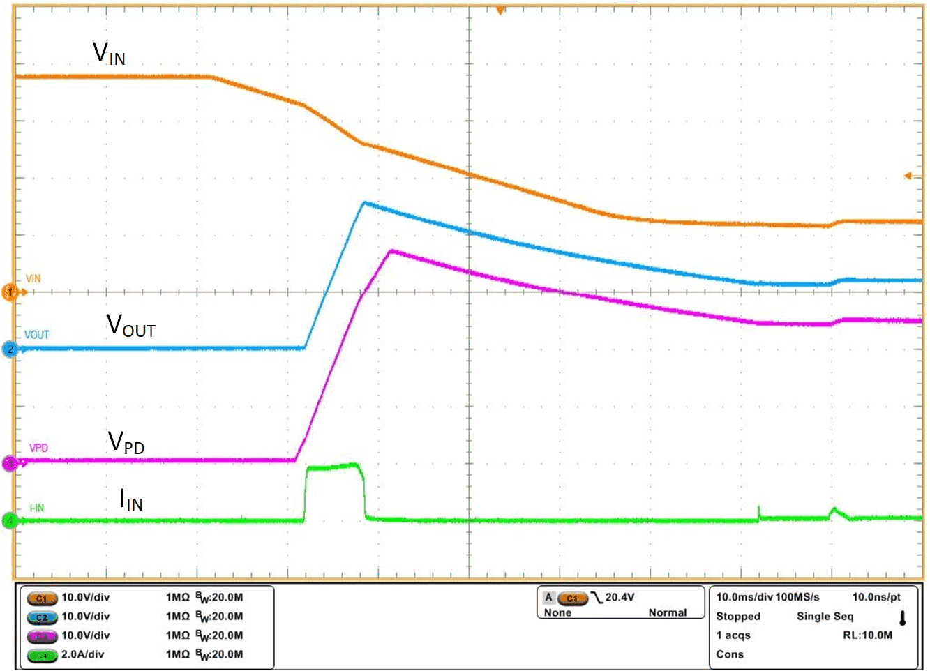 Figure 9-17 Overvoltage
Recovery
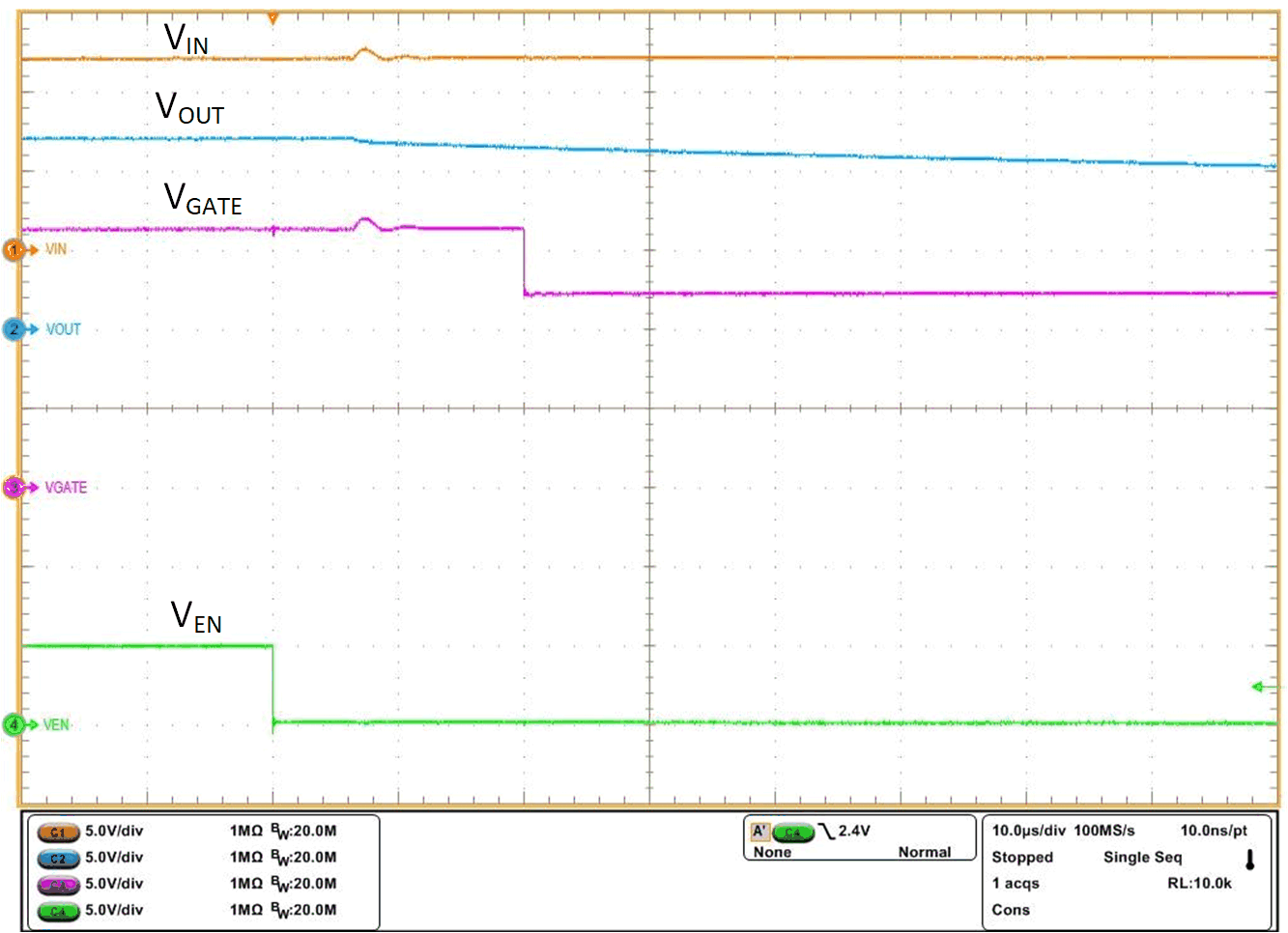 Figure 9-19 Turn-off Delay –
GATE
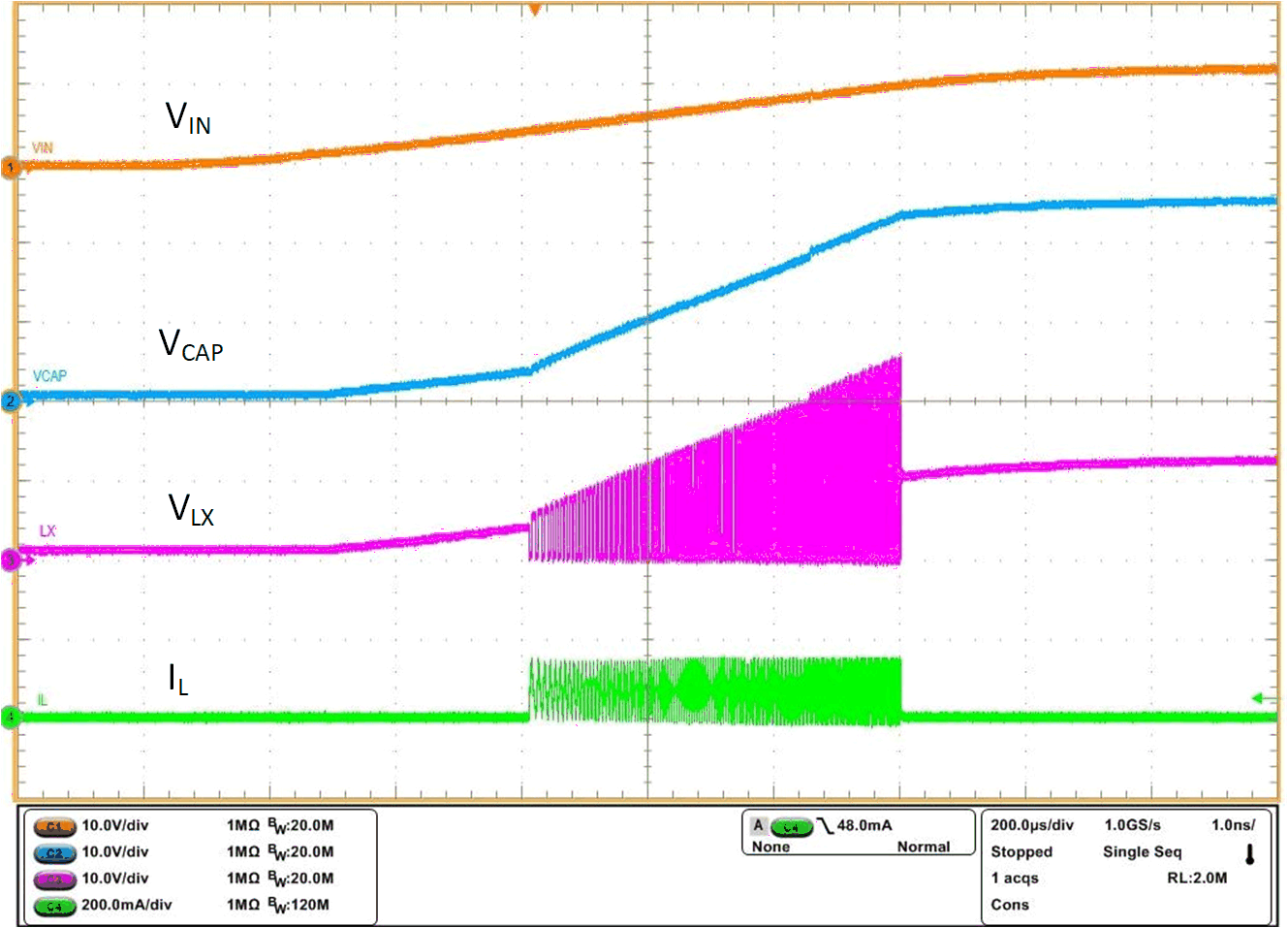 Figure 9-8 Start-up 12 V Showing
Boost Output (VCAP) and Switching (VLX)
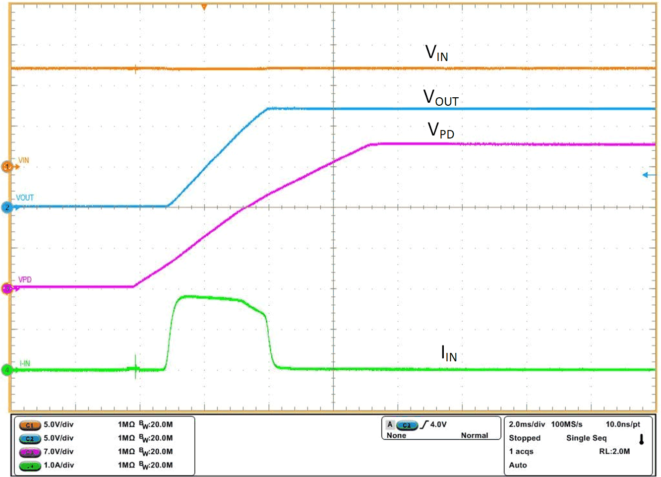 Figure 9-10 Inrush Current with No
Load at Output
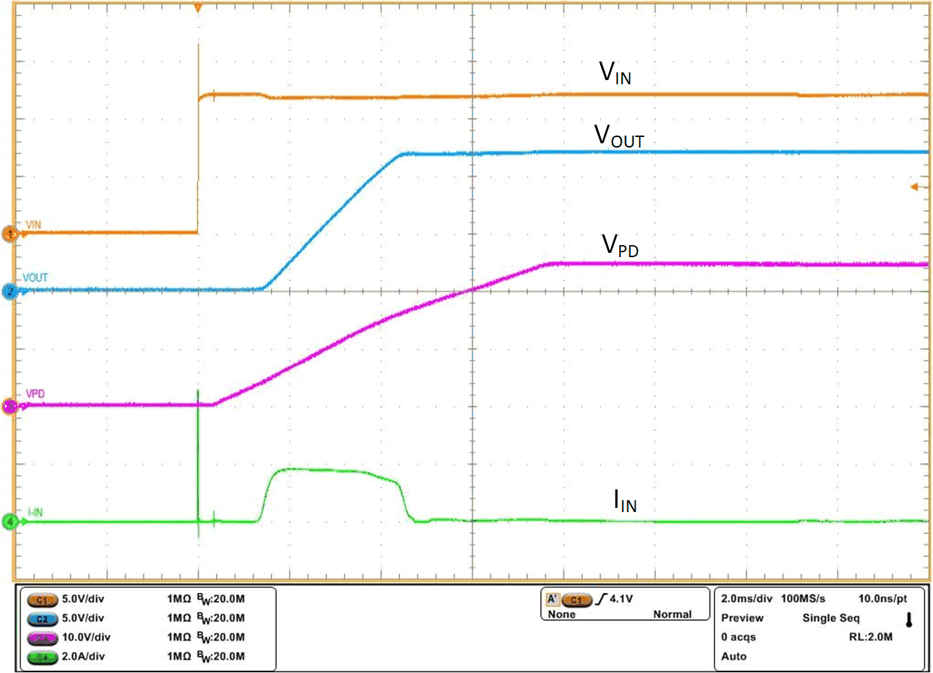 Figure 9-12 Hot-Plug into 12 V
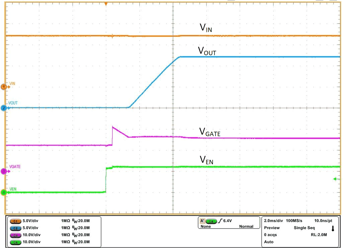 Figure 9-14 GATE Turn-on with
Enable
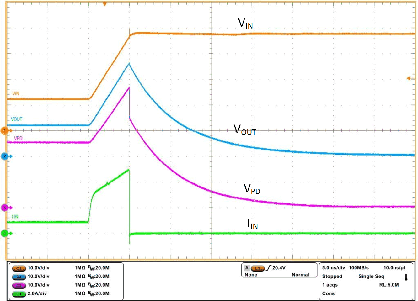 Figure 9-16 Overvoltage
Protection
 Figure 9-18 Turn-on Delay – PD
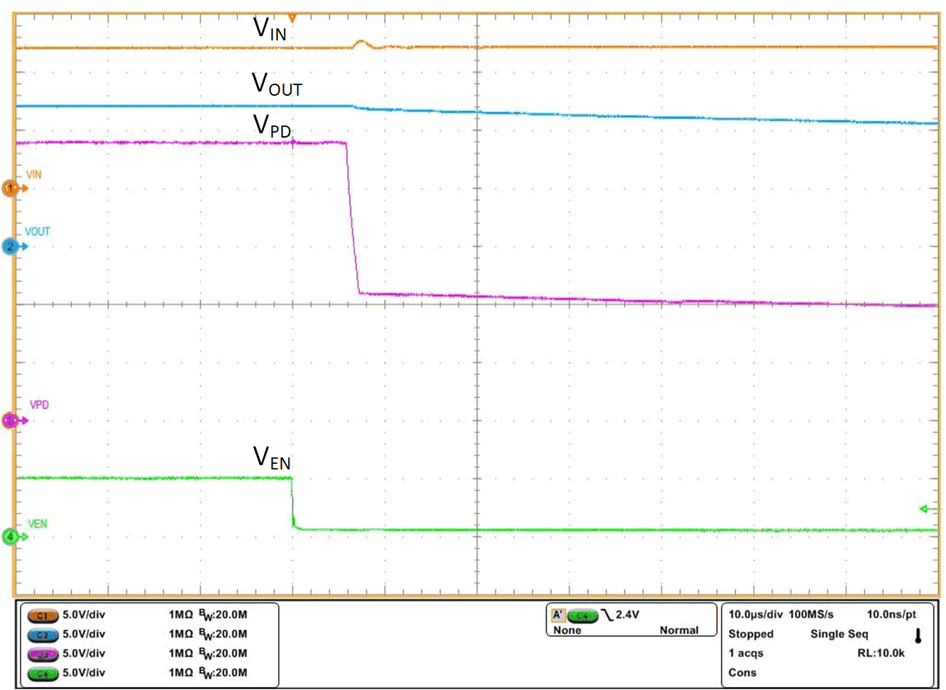 Figure 9-20 Turn-off Delay –
PD