ZHCSLA3A May 2020 – December 2020 LM7481-Q1
PRODUCTION DATA
- 1 特性
- 2 应用
- 3 说明
- 4 Revision History
- 5 Pin Configuration and Functions
- 6 Specifications
- 7 Parameter Measurement Information
- 8 Detailed Description
-
9 Application and Implementation
- 9.1 Application Information
- 9.2
Typical 12-V Reverse Battery Protection Application
- 9.2.1 Design Requirements for 12-V Battery Protection
- 9.2.2 Automotive Reverse Battery Protection
- 9.2.3 Input Transient Protection: ISO 7637-2 Pulse 1
- 9.2.4 AC Super Imposed Input Rectification: ISO 16750-2 and LV124 E-06
- 9.2.5 Input Micro-Short Protection: LV124 E-10
- 9.2.6 Detailed Design Procedure
- 9.2.7 MOSFET Selection: Blocking MOSFET Q1
- 9.2.8 MOSFET Selection: Hot-Swap MOSFET Q2
- 9.2.9 TVS selection
- 9.2.10 Application Curves
- 9.3 Do's and Don'ts
- 10Power Supply Recommendations
- 11Layout
- 12Device and Documentation Support
- 13Mechanical, Packaging, and Orderable Information
8.3.2.1 Reverse Battery Protection (A, C, DGATE)
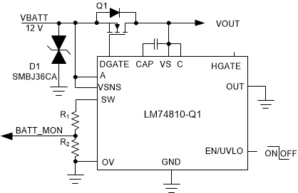
A, C, DGATE comprises of Ideal Diode stage. Connect the Source of the external MOSFET to A, Drain to C and Gate to DGATE. The LM74810-Q1 has integrated reverse input protection down to –65 V.
Before the DGATE driver is enabled, following conditions must be achieved:
- The EN/UVLO pin voltage must be greater than the specified input high voltage.
- The CAP to VS voltage must be greater than the undervoltage lockout voltage.
- Voltage at A pin must be greater than VA POR Rising threshold.
- Voltage at Vs pin must be greater than Vs POR Rising thershold.
In LM74810-Q1 the voltage drop across the MOSFET is continuously monitored between the A and C pins, and the DGATE to A voltage is adjusted as needed to regulate the forward voltage drop at 9.1 mV (typ). This closed loop regulation scheme enables graceful turn off of the MOSFET during a reverse current event and ensures zero DC reverse current flow. This scheme ensures robust performance during slow input voltage ramp down tests. Along with the linear regulation amplifier scheme, the LM74810-Q1 also integrates a fast reverse voltage comparator. When the voltage drop across A and C reaches V(AC_REV) threshold then the DGATE goes low within 0.5-µs (typ). This fast reverse voltage comparator scheme ensures robust performance during fast input voltage ramp down tests such as input micro-shorts. The external MOSFET is turned ON back when the voltage across A and C hits V(AC_FWD) threshold within 0.85 µs (typ).
For Ideal Diode only designs, connect LM74810-Q1 as shown in Figure 8-2.
 Figure 8-2 Configuring LM74810-Q1 for Ideal Diode Only