ZHCSH62B December 2017 – October 2019 LM76002-Q1 , LM76003-Q1
PRODUCTION DATA.
- 1 特性
- 2 应用
- 3 说明
- 4 修订历史记录
- 5 Pin Configuration and Functions
- 6 Specifications
-
7 Detailed Description
- 7.1 Overview
- 7.2 Functional Block Diagram
- 7.3
Feature Description
- 7.3.1 Fixed-Frequency, Peak-Current-Mode Control
- 7.3.2 Light Load Operation Modes — PFM and FPWM
- 7.3.3 Adjustable Output Voltage
- 7.3.4 Enable (EN Pin) and UVLO
- 7.3.5 Internal LDO, VCC UVLO, and Bias Input
- 7.3.6 Soft Start and Voltage Tracking (SS/TRK)
- 7.3.7 Adjustable Switching Frequency (RT) and Frequency Synchronization
- 7.3.8 Minimum On-Time, Minimum Off-Time, and Frequency Foldback at Dropout Conditions
- 7.3.9 Internal Compensation and CFF
- 7.3.10 Bootstrap Voltage and VBOOT UVLO (BOOT Pin)
- 7.3.11 Power Good and Overvoltage Protection (PGOOD)
- 7.3.12 Overcurrent and Short-Circuit Protection
- 7.3.13 Thermal Shutdown
- 7.4 Device Functional Modes
-
8 Application and Implementation
- 8.1 Application Information
- 8.2
Typical Applications
- 8.2.1 Design Requirements
- 8.2.2
Detailed Design Procedure
- 8.2.2.1 Custom Design With WEBENCH® Tools
- 8.2.2.2 Output Voltage Setpoint
- 8.2.2.3 Switching Frequency
- 8.2.2.4 Input Capacitors
- 8.2.2.5 Inductor Selection
- 8.2.2.6 Output Capacitor Selection
- 8.2.2.7 Feed-Forward Capacitor
- 8.2.2.8 Bootstrap Capacitors
- 8.2.2.9 VCC Capacitors
- 8.2.2.10 BIAS Capacitors
- 8.2.2.11 Soft-Start Capacitors
- 8.2.2.12 Undervoltage Lockout Setpoint
- 8.2.2.13 PGOOD
- 8.2.2.14 Synchronization
- 8.2.3 Application Curves
- 9 Power Supply Recommendations
- 10Layout
- 11器件和文档支持
- 12机械、封装和可订购信息
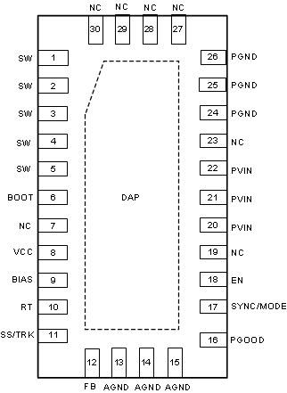
5 Pin Configuration and Functions
RNP Package
30-Pin WQFN
Top View

Pin Functions
| PIN | I/O(1) | DESCRIPTION | |
|---|---|---|---|
| NO. | NAME | ||
| 1, 2, 3, 4, 5 | SW | P | Switching output of the regulator. Internally connected to source of the HS FET and drain of the LS FET. Connect to power inductor and boot-strap capacitor. |
| 6 | BOOT | P | Boot-strap capacitor connection for high-side driver. Connect a high-quality 470-nF capacitor from this pin to the SW pin. |
| 7, 19, 23, 27, 28, 29, 30 | NC | — | Not internally connected. Connect to ground copper on PCB to improve heat-sinking of the device and board level reliability. |
| 8 | VCC | P | Output of internal bias supply. Used as supply to internal control circuits. Connect a high-quality 2.2-µF capacitor from this pin to GND. TI does not recommended loading this pin by external circuitry. |
| 9 | BIAS | P | Optional BIAS LDO supply input. TI recommends tying this to VOUT when 3.3 V ≤ VOUT ≤ 18 V, or tying to an external 3.3-V or 5-V rail if available, to improve efficiency. When used, place a 1-µF capacitor from this terminal to ground. Tie to ground when not in use. |
| 10 | RT | A | Switching frequency setting pin. Place a resistor from this pin to ground to set the switching frequency. If floating, the default switching frequency is 500 kHz. Do not short to ground. |
| 11 | SS/TRK | A | Soft-start-control pin. Leave this pin floating to use the 6.3-ms internal soft-start ramp. An external capacitor can be connected from this pin to ground to extend the soft-start time. A 2-µA current sourced from this pin can charge the capacitor to provide the ramp. Connect to external ramp for tracking. Do not short to ground. |
| 12 | FB | A | Feedback input for output voltage regulation. Connect a resistor divider to set the output voltage. Never short this terminal to ground during operation. |
| 16 | PGOOD | A | Open-drain power-good flag output. Connect to suitable voltage supply through a current limiting resistor. High = VOUT regulation OK, Low = VOUT regulation fault. PGOOD = Low when EN = Low. |
| 17 | SYNC/MODE | A | Synchronization input and mode setting pin. Do not float, tie to ground if not used. Tie to ground: DCM/PFM operation under light loads, improved efficiency; tie to logic high: forced PWM under light loads, constant switching frequency over load; tie to external clock source: synchronize switching action to the clock, forced PWM under light loads. Triggers on the rising edge of external clock. |
| 18 | EN | A | Precision-enable input to regulator. Do not float. High = on, Low = off. Can be tied to VIN. Precision-enable input allows adjustable UVLO by external resistor divider. |
| 13, 14, 15 | AGND | G | Analog ground. Ground reference for internal references and logic. All electrical parameters are measured with respect to this pin. Connect to system ground on PCB. |
| 20, 21, 22 | PVIN | P | Supply input to internal bias LDO and HS FET. Connect to input supply and input bypass capacitors CIN. CIN must be placed right next to this pin and PGND and connected with short traces. |
| 24, 25, 26 | PGND | G | Power ground, connected to the source of LS FET internally. Connect to system ground, DAP/EP, AGND, ground side of CIN and COUT. Path to CIN must be as short as possible. |
| EP | DAP | — | Low impedance connection to AGND. Connect to system ground on PCB. Major heat dissipation path for the die. Must be used for heat sinking by soldering to ground copper on PCB. Thermal vias are preferred. |
(1) A = Analog, O = Output, I = Input, G = Ground, P = Power