ZHCSH05A October 2017 – October 2019 LM76002 , LM76003
PRODUCTION DATA.
- 1 特性
- 2 应用
- 3 说明
- 4 修订历史记录
- 5 Pin Configuration and Functions
- 6 Specifications
-
7 Detailed Description
- 7.1 Overview
- 7.2 Functional Block Diagram
- 7.3
Feature Description
- 7.3.1 Fixed-Frequency, Peak-Current-Mode Control
- 7.3.2 Light Load Operation Modes — PFM and FPWM
- 7.3.3 Adjustable Output Voltage
- 7.3.4 Enable (EN Pin) and UVLO
- 7.3.5 Internal LDO, VCC UVLO, and Bias Input
- 7.3.6 Soft Start and Voltage Tracking (SS/TRK)
- 7.3.7 Adjustable Switching Frequency (RT) and Frequency Synchronization
- 7.3.8 Minimum On-Time, Minimum Off-Time, and Frequency Foldback at Dropout Conditions
- 7.3.9 Internal Compensation and CFF
- 7.3.10 Bootstrap Voltage and VBOOT UVLO (BOOT Pin)
- 7.3.11 Power Good and Overvoltage Protection (PGOOD)
- 7.3.12 Overcurrent and Short-Circuit Protection
- 7.3.13 Thermal Shutdown
- 7.4 Device Functional Modes
-
8 Application and Implementation
- 8.1 Application Information
- 8.2
Typical Applications
- 8.2.1 Design Requirements
- 8.2.2
Detailed Design Procedure
- 8.2.2.1 Custom Design With WEBENCH® Tools
- 8.2.2.2 Output Voltage Setpoint
- 8.2.2.3 Switching Frequency
- 8.2.2.4 Input Capacitors
- 8.2.2.5 Inductor Selection
- 8.2.2.6 Output Capacitor Selection
- 8.2.2.7 Feed-Forward Capacitor
- 8.2.2.8 Bootstrap Capacitors
- 8.2.2.9 VCC Capacitors
- 8.2.2.10 BIAS Capacitors
- 8.2.2.11 Soft-Start Capacitors
- 8.2.2.12 Undervoltage Lockout Setpoint
- 8.2.2.13 PGOOD
- 8.2.2.14 Synchronization
- 8.2.3 Application Curves
- 9 Power Supply Recommendations
- 10Layout
- 11器件和文档支持
- 12机械、封装和可订购信息
8.2 Typical Applications
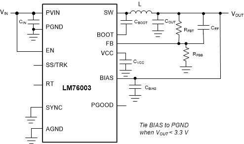
The LM76002/LM76003 only requires a few external components to convert from a wide range of supply voltage to output voltage, as shown in Figure 21:
 Figure 21. LM76002/LM76003 Basic Schematic
 The LM76002/LM76003 also integrates a full list of features to aid system design requirements, such as VCC UVLO, programmable soft start, start-up tracking, programmable switching frequency, clock synchronization, and a power-good indication. Each system can select the features needed in a specific application. A comprehensive schematic with all features utilized is shown in Figure 22:
 Figure 22. LM76002/LM76003 Comprehensive Schematic
 The external components must fulfill the requirements of the application, but also the stability criteria of the device control loop. The LM76002/LM76003 is optimized to work within a range of external components. Inductance and capacitance of the LC output filter each create poles that have to be considered in the control of the converter. Table 2 can be used to simplify the output filter component selection.
Table 2. Typical Component Selection
| fSW (kHz) | VOUT (V) | L (µH) | COUT (µF) | RFBT (kΩ) | RFBB (kΩ) |
| 300 | 1 | 2.5 | 680 | 100 | OPEN |
| 500 | 1 | 1.5 | 470 | 100 | OPEN |
| 1000 | 1 | 0.68 | 200 | 100 | OPEN |
| 2200 | 1 | 0.47 | 120 | 100 | OPEN |
| 300 | 3.3 | 6.8 | 200 | 100 | 43.5 |
| 500 | 3.3 | 4.7 | 150 | 100 | 43.5 |
| 1000 | 3.3 | 2.5 | 88 | 100 | 43.5 |
| 2200 | 3.3 | 1.2 | 44 | 100 | 43.5 |
| 300 | 5 | 10 | 150 | 100 | 25 |
| 500 | 5 | 6.8 | 100 | 100 | 25 |
| 1000 | 5 | 3.3 | 66 | 100 | 25 |
| 2200 | 5 | 1.5 | 44 | 100 | 25 |
| 300 | 12 | 22 | 66 | 100 | 9.09 |
| 500 | 12 | 15 | 44 | 100 | 9.09 |
| 1000 | 12 | 6.8 | 22 | 100 | 9.09 |
| 2200 | 12 | 3.3 | 22 | 100 | 9.09 |
| 300 | 24 | 47 | 40 | 100 | 4.37 |
| 500 | 24 | 27 | 33 | 100 | 4.37 |
| 1000 | 24 | 15 | 22 | 100 | 4.37 |
| 2200 | 24 | 6.8 | 22 | 100 | 4.37 |