ZHCSJE7A March 2019 – September 2019 LM76202-Q1
PRODUCTION DATA.
- 1 特性
- 2 应用
- 3 说明
- 4 修订历史记录
- 5 Pin Configuration and Functions
- 6 Specifications
- 7 Parameter Measurement Information
-
8 Detailed Description
- 8.1 Overview
- 8.2 Functional Block Diagram
- 8.3
Feature Description
- 8.3.1 Undervoltage Lockout (UVLO)
- 8.3.2 Overvoltage Protection (OVP)
- 8.3.3 Reverse Battery Protection
- 8.3.4 Hot Plug-In and In-Rush Current Control
- 8.3.5 Overload and Short Circuit Protection
- 8.4 Device Functional Modes
-
9 Application and Implementation
- 9.1 Application Information
- 9.2
Typical Application
- 9.2.1 Design Requirements
- 9.2.2 Detailed Design Procedure
- 9.2.3 Application Curves
- 10Power Supply Recommendations
- 11Layout
- 12器件和文档支持
- 13机械、封装和可订购信息
8.3.2 Overvoltage Protection (OVP)
The device incorporates circuitry to protect the system during overvoltage conditions. This device features an overvoltage cut off functionality. A voltage more than V(OVPR) on OVP pin turns off the internal FET and protects the downstream load. To program the OVP threshold, connect a resistor divider from IN supply to OVP terminal to RTN as shown in Figure 21. OVP Overvoltage Cut-off response is shown in Figure 22. OVP pin must not be left floating. If OVP pin could be floating due to dry soldering, an additional zener diode at the output will be required for protection from over voltage.
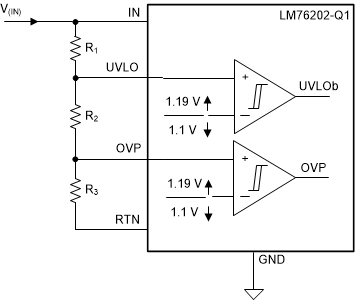 Figure 21. OVP Threshold Setting
 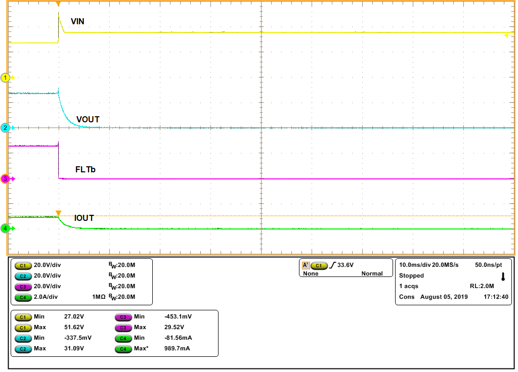 Figure 22. OVP Overvoltage Cut-Off
 Programmable overvoltage clamp can also be achieved using LM76202-Q1 by connecting the resistor ladder from Vout to OVP to RTN as shown in Figure 23 . This results in clamping of output voltage close to OVP set-point by resistors R1 and R2. as shown in Figure 24. This scheme will also help in achieving minimal system Iq during off state. For this OVP configurataion, use R1 > 90 kΩ.
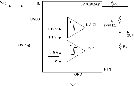
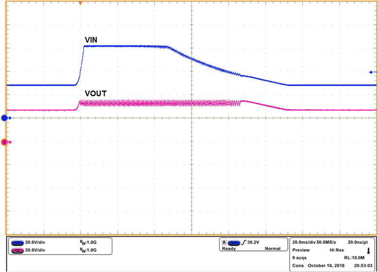 Figure 24. Programmable Overvoltage Clamp Response
 The LM76202-Q1 device also features an internally fixed 38 V overvoltage clamp (VOVC) functionality. The OVP terminal of theLM76202-Q1 device must be connected to the RTN terminal directly as shown in Figure 25. The LM76202-Q1 clamps the output voltage to VOVC, when the input voltage exceeds 38 V. During the output voltage clamp operation, the power dissipation in the internal MOSFET is PD = (VIN – VOVC) × IOUT. Excess power dissipation for prolonged period can make the device to enter into thermal shutdown. Figure 26 illustrates the overvoltage clamp functionality.
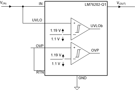 Figure 25. Internal Fixed OV Clamp Setting
 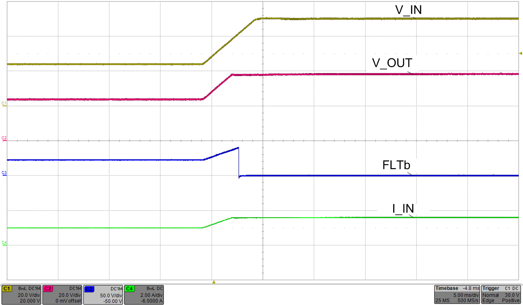 Figure 26. Internal OV Clamp Response