ZHCSI84D November   2008  – May 2018 LM7705

PRODUCTION DATA.  

  1. 特性
  2. 应用
  3. 说明
    1.     Device Images
      1.      典型应用
  4. 修订历史记录
  5. Pin Configuration and Functions
    1.     Pin Functions
  6. Specifications
    1. 6.1 Absolute Maximum Ratings
    2. 6.2 ESD Ratings
    3. 6.3 Recommended Operating Conditions
    4. 6.4 Thermal Information
    5. 6.5 3.3-V Electrical Characteristics
    6. 6.6 5-V Electrical Characteristics
    7. 6.7 Typical Characteristics
  7. Detailed Description
    1. 7.1 Overview
    2. 7.2 Functional Block Diagram
    3. 7.3 Feature Description
      1. 7.3.1 Supply Voltage
      2. 7.3.2 Output Voltage and Line Regulation
      3. 7.3.3 Output Current and Load Regulation
      4. 7.3.4 Quiescent Current
    4. 7.4 Device Functional Modes
      1. 7.4.1 General Amplifier Application
        1. 7.4.1.1 One-Stage, Single-Supply True Zero Amplifier
        2. 7.4.1.2 Two-Stage, Single-Supply True Zero Amplifier
        3. 7.4.1.3 Dual-Supply, True Zero Amplifiers
  8. Application and Implementation
    1. 8.1 Application Information
      1. 8.1.1 Functional Description
      2. 8.1.2 Technical Description
      3. 8.1.3 Charge Pump Theory
    2. 8.2 Typical Application
      1. 8.2.1 Design Requirements
      2. 8.2.2 Detailed Design Procedure
        1. 8.2.2.1 Basic Setup
      3. 8.2.3 Application Curves
  9. Power Supply Recommendations
  10. 10Layout
    1. 10.1 Layout Guidelines
    2. 10.2 Layout Examples
  11. 11器件和文档支持
    1. 11.1 社区资源
    2. 11.2 商标
    3. 11.3 静电放电警告
    4. 11.4 术语表
  12. 12机械、封装和可订购信息

封装选项

机械数据 (封装 | 引脚)
散热焊盘机械数据 (封装 | 引脚)
订购信息

Charge Pump Theory

This section uses a simplified but realistic equivalent circuit that represents the basic function of the charge pump. The schematic is given in Figure 30.
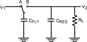
LM7705 20173033.gifFigure 30. Charge Pump

When the switch is in position A, capacitor CFLY will charge to voltage V1. The total charge on capacitor CFLY is Q1 = CFLY × V 1. The switch then moves to position B, discharging CFLY to voltage V2. After this discharge, the charge on CFLY will be Q2 = CFLY × V2. The charge has been transferred from the source V1 to the output V2. The amount of charge transferred is:

Equation 1. LM7705 20173037.gif

When the switch changes between A and B at a frequency f, the charge transfer per unit time, or current is:

Equation 2. LM7705 20173038.gif

The switched capacitor network can be replaced by an equivalent resistor, as indicated in Figure 31.
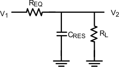
LM7705 20173032.gifFigure 31. Switched Capacitor Equivalent Circuit

The value of this resistor is dependent on both the capacitor value and the switching frequency as given in Equation 3

Equation 3. LM7705 20173039.gif

The value for REQ can be calculated from Equation 3 and is given in Equation 4

Equation 4. LM7705 20173048.gif

Equation 4 show that the value for the resistance at an increased internal switching frequency, allows a lower value for the used capacitor.