SNVS090G May 2004 – June 2020 LM341
PRODUCTION DATA.
- 1 Features
- 2 Applications
- 3 Description
- 4 Revision History
- 5 Device Comparison Table
- 6 Pin Configuration and Functions
- 7 Specifications
- 8 Detailed Description
- 9 Application and Implementation
- 10Power Supply Recommendations
- 11Layout
- 12Device and Documentation Support
- 13Mechanical, Packaging, and Orderable Information
11.1.1 Thermal Considerations
When an integrated circuit operates with appreciable current, its junction temperature is elevated. It is important to quantify its thermal limits to achieve acceptable performance and reliability. This limit is determined by summing the individual parts consisting of a series of temperature rises from the semiconductor junction to the operating environment. A one-dimension steady-state model of conduction heat transfer is demonstrated in Figure 15. The heat generated at the device junction flows through the die to the die attach pad, through the lead frame to the surrounding case material, to the printed-circuit board, and eventually to the ambient environment.
There are several variables that may affect the thermal resistance and in turn the need for a heat sink, which includes the following.
Component variables (RθJC)
- Leadframe size and material
- Number of conduction pins
- Die size
- Die attach material
- Molding compound size and material
Application variables (RθCA)
- Mounting pad size, material, and location
- Placement of mounting pad
- PCB size and material
- Traces length and width
- Adjacent heat sources
- Volume of air
- Ambient temperature
- Shape of mounting pad

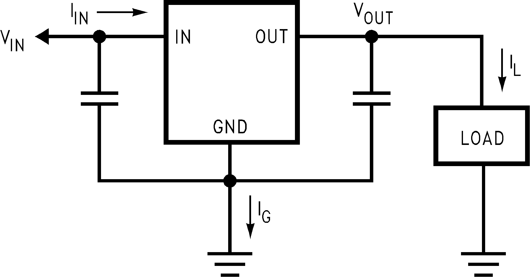
The LM341 and LM78M05 regulators have internal thermal shutdown to protect the device from overheating. Under all possible operating conditions, the junction temperature of the LM341 and LM78M05 must be within the range of 0°C to 125°C. A heat sink may be required depending on the maximum power dissipation and maximum ambient temperature of the application. To determine if a heat sink is needed, the power dissipated by the regulator (PD) is calculated using Equation 1.
Figure 16 shows the voltages and currents which are present in the circuit.
 Figure 16. Power Dissipation Diagram
 The next parameter which must be calculated is the maximum allowable temperature rise, TR(MAX).
where
- TJ(MAX) is the maximum allowable junction temperature (125°C)
- TA(MAX) is the maximum ambient temperature encountered in the application
Using the calculated values for TR(MAX) and PD, the maximum allowable value for the junction-to-ambient thermal resistance (RθJA) can be calculated with Equation 3.
As a design aid, Table 2 lists the value of the RθJA of TO-252 for different heat sink area. The copper patterns that we used to measure these RθJA are shown at the end of the AN–1028 Maximum Power Enhancement Techniques for Power Packages application note. Figure 12 reflects the same test results as what are in the Table 2.
Figure 13 illustrates the maximum allowable power dissipation versus ambient temperature for the PFM device. Figure 14 illustrates the maximum allowable power dissipation versus copper area (in2) for the TO-252 device. For power enhancement techniques to be used with TO-252 package, see the AN–1028 Maximum Power Enhancement Techniques for Power Packages application note.
Table 2. RθJA Different Heat Sink Area
| LAYOUT | COPPER AREA (in2) | THERMAL RESISTANCE: RθJA (°C/W) | |
|---|---|---|---|
| TOP SIDE(1) | BOTTOM SIDE | TO-252 | |
| 1 | 0.0123 | 0 | 103 |
| 2 | 0.066 | 0 | 87 |
| 3 | 0.3 | 0 | 60 |
| 4 | 0.53 | 0 | 54 |
| 5 | 0.76 | 0 | 52 |
| 6 | 1 | 0 | 47 |
| 7 | 0 | 0.2 | 84 |
| 8 | 0 | 0.4 | 70 |
| 9 | 0 | 0.6 | 63 |
| 10 | 0 | 0.8 | 57 |
| 11 | 0 | 1 | 57 |
| 12 | 0.066 | 0.066 | 89 |
| 13 | 0.175 | 0.175 | 72 |
| 14 | 0.284 | 0.284 | 61 |
| 15 | 0.392 | 0.392 | 55 |
| 16 | 0.5 | 0.5 | 53 |