SNOS975G May 2001 – August 2015 LM8262
PRODUCTION DATA.
1 Features
- GBWP 21MHz
- Wide Supply Voltage Range 2.5 V to 22 V
- Slew Rate 12V/µs
- Supply Current/channel 1.15 mA
- Cap Load Limit Unlimited
- Output Short Circuit Current +53mA/−75 mA
- +/−5% Settling Time 400ns (500 pF, 100 mVPP step)
- Input Common Mode Voltage 0.3 V Beyond Rails
- Input Voltage Noise 15nV/√Hz
- Input Current Noise 1pA/√Hz
- THD+N < 0.05%
(VS = 5V, TA = 25°C, Typical Values Unless Specified).
2 Applications
- TFT‐LCD Flat Panel VCOM driver
- A/D Converter Buffer
- High Side/low Side Sensing
- Headphone Amplifier
3 Description
The LM8262 is a Rail-to-Rail input and output Op Amp which can operate with a wide supply voltage range. This device has high output current drive, greater than Rail-to-Rail input common mode voltage range, unlimited capacitive load drive capability, and provides tested and ensured high speed and slew rate. It is specifically designed to handle the requirements of flat panel TFT panel VCOM driver applications as well as being suitable for other low power and medium speed applications which require ease of use and enhanced performance over existing devices.
Greater than Rail-to-Rail input common mode voltage range with 50 dB of Common Mode Rejection allows high side and low side sensing for many applications without concern for exceeding the range and with no compromise in accuracy. In addition, most device parameters are insensitive to power supply variations. This design enhancement is yet another step in simplifying its usage. The output stage has low distortion (0.05% THD+N) and can supply a respectable amount of current (15 mA) with minimal headroom from either rail (300 mV).
The LM8262 is offered in the space saving VSSOP package.
Device Information(1)
| PART NUMBER | PACKAGE | BODY SIZE (NOM) |
|---|---|---|
| LM8262 | VSSOP (8) | 3.00 mm × 3.00 mm |
- For all available packages, see the orderable addendum at the end of the datasheet.
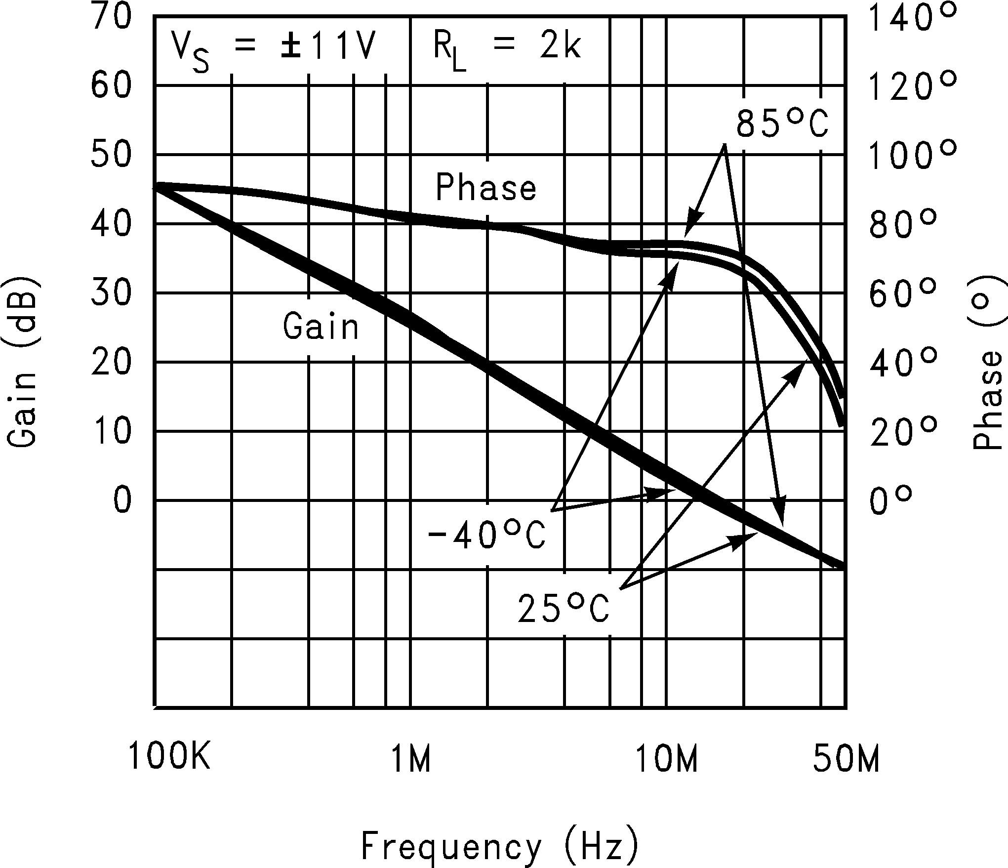
Gain/Phase vs. Frequency

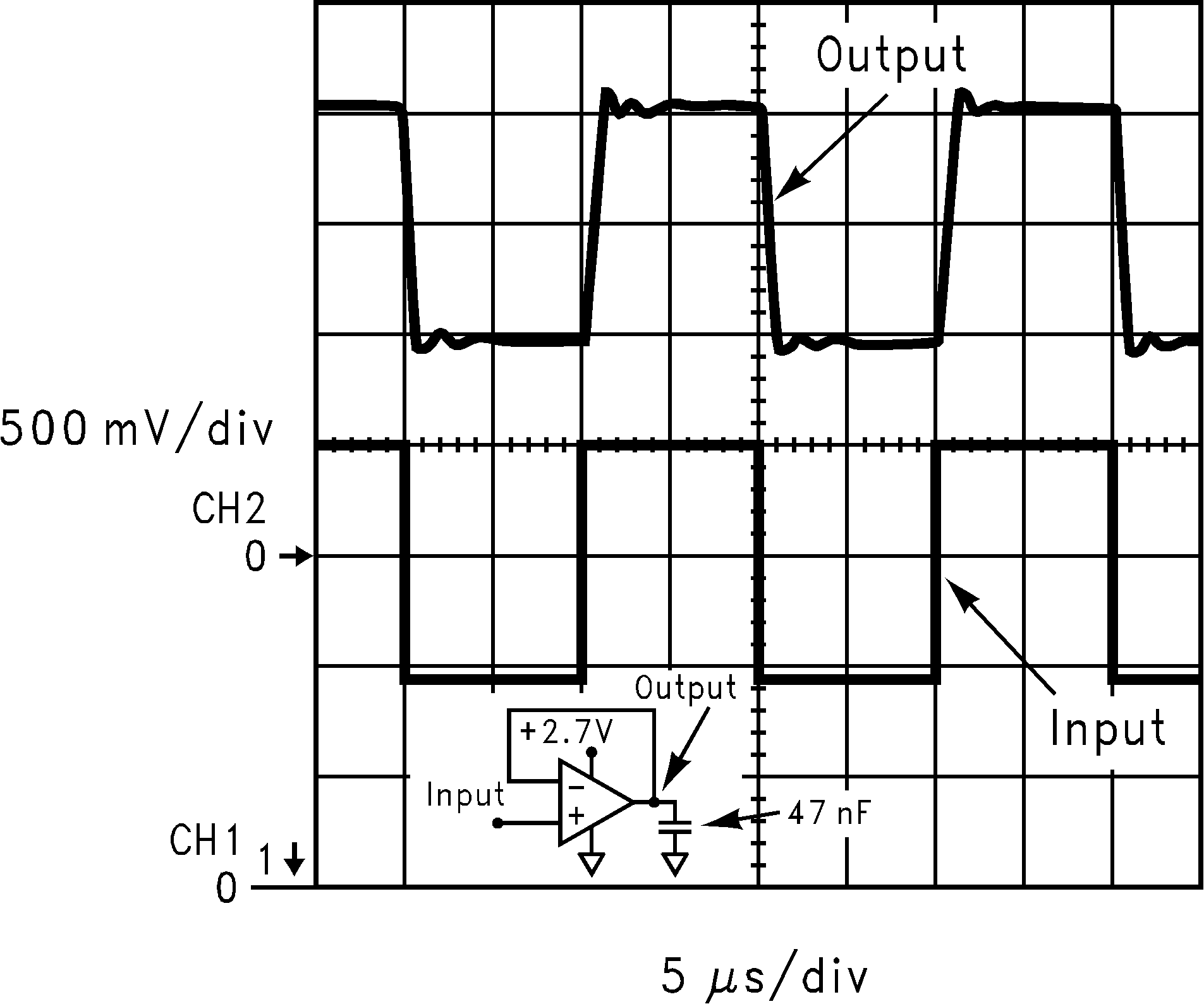
Output Response with Heavy Capacitive Load
