SNVS233C March 2003 – December 2015 LM8365
PRODUCTION DATA.
6 Specifications
6.1 Absolute Maximum Ratings
See (1)(2).| MIN | MAX | UNIT | ||
|---|---|---|---|---|
| Supply voltage | −0.3 | 6.5 | V | |
| RESET output voltage | −0.3 | 6.5 | V | |
| RESET output current | 70 | mA | ||
| Mounting temperature | Lead temp. (soldering 10 sec) | 260 | °C | |
| Junction temperature | 125 | °C | ||
| Storage temperature, Tstg | −65 | 150 | °C | |
(1) Stresses beyond those listed under Absolute Maximum Ratings may cause permanent damage to the device. These are stress ratings only, which do not imply functional operation of the device at these or any other conditions beyond those indicated under Recommended Operating Conditions. Exposure to absolute-maximum-rated conditions for extended periods may affect device reliability.
(2) If Military/Aerospace specified devices are required, please contact the Texas Instruments Sales Office/Distributors for availability and specifications.
6.2 ESD Ratings
| VALUE | UNIT | |||
|---|---|---|---|---|
| V(ESD) | Electrostatic discharge | Human-body model (HBM), per ANSI/ESDA/JEDEC JS-001(1) | ±2000 | V |
| Charged-device model (CDM), per JEDEC specification JESD22-C101(2) | ±200 | |||
(1) JEDEC document JEP155 states that 500-V HBM allows safe manufacturing with a standard ESD control process. Manufacturing with less than 500-V HBM is possible with the necessary precautions. Pins listed as ±2000 V may actually have higher performance.
(2) JEDEC document JEP157 states that 250-V CDM allows safe manufacturing with a standard ESD control process. Manufacturing with less than 250-V CDM is possible with the necessary precautions. Pins listed as ±200 V may actually have higher performance.
6.3 Recommended Operating Conditions(1)
| MIN | MAX | UNIT | |
|---|---|---|---|
| Temperature | −40 | 85 | °C |
(1) Absolute Maximum Ratings indicate limits beyond which damage to the device may occur. Recommended Operating Conditions indicate conditions for which the device is intended to be functional, but specific performance is not ensured. For ensured specifications and the test conditions, see the Electrical Characteristics.
6.4 Thermal Information
| THERMAL METRIC(1) | LM8365 | UNIT | |
|---|---|---|---|
| DBV (SOT-23) | |||
| 5 PINS | |||
| RθJA | Junction-to-ambient thermal resistance | 191.1 | °C/W |
| RθJC(top) | Junction-to-case (top) thermal resistance | 144.6 | °C/W |
| RθJB | Junction-to-board thermal resistance | 35.9 | °C/W |
| ψJT | Junction-to-top characterization parameter | 31.1 | °C/W |
| ψJB | Junction-to-board characterization parameter | 35.3 | °C/W |
| RθJC(bot) | Junction-to-case (bottom) thermal resistance | — | °C/W |
(1) For more information about traditional and new thermal metrics, see the Semiconductor and IC Package Thermal Metrics application report, SPRA953.
6.5 Electrical Characteristics
Unless otherwise specified, all limits specified for TA = 25°C.| PARAMETER | TEST CONDITIONS | MIN(2) | TYP(1) | MAX(2) | UNIT | ||
|---|---|---|---|---|---|---|---|
| VDET− | Detector threshold voltage | High-to-low state output (VIN decreasing) |
27 suffix | 2.633 | 2.7 | 2.767 | V |
| 45 suffix | 4.388 | 4.5 | 4.613 | ||||
| VHYS | Detector threshold hysteresis | VIN increasing | 27 suffix | 0.081 | 0.135 | 0.189 | V |
| 45 suffix | 0.135 | 0.225 | 0.315 | ||||
| ΔVdet/ΔT | Detector threshold voltage temperature coefficient | ±100 | PPM/°C | ||||
| VOL | RESET output voltage | Open-drain ISINK = 1 mA |
0.25 | 0.5 | V | ||
| IOL | RESET output sink current | VIN = 1.5 V, VOL = 0.5 V | 1 | 2.5 | mA | ||
| IOH | RESET output source current | VIN = 4.5 V, VOL = 2.4 V | 1 | 7 | mA | ||
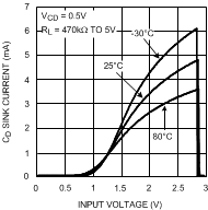
| ICD | Delay pin output sink current | VIN = 1.5 V, VCD = 0.5 V | 0.2 | 1.8 | mA | ||
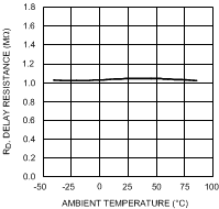
| RD | Delay resistance | 0.5 | 1 | 2 | MΩ | ||
| VIN | Operating input voltage range | 1 | 6 | V | |||
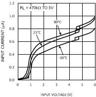
| IIN | Quiescent input current | 27 suffix | VIN = 2.6 V | 0.62 | 0.9 | μA | |
| VIN = 4.7 V | 0.75 | 1.3 | |||||
| 45 suffix | VIN = 4.34 V | 0.7 | 1 | ||||
| VIN = 6 V | 0.85 | 1.4 | |||||
(1) Typical values represent the most likely parametric norm.
(2) All limits are specified by testing or statistical analysis.
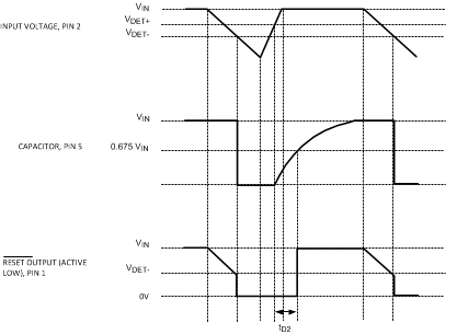 Figure 1. Timing Waveforms
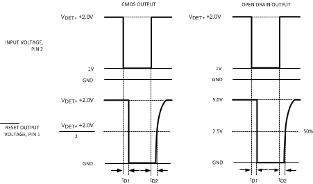 Figure 2. Propagation Delay Timing Diagrams
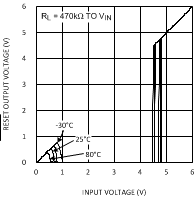
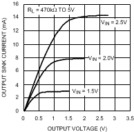
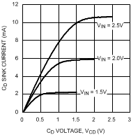
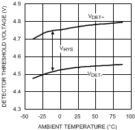
6.6 Typical Characteristics
