SNIS146B March 2007 – October 2017 LM95214
PRODUCTION DATA.
- 1 Features
- 2 Applications
- 3 Description
- 4 Revision History
- 5 Pin Configuration and Functions
-
6 Specifications
- 6.1 Absolute Maximum Ratings
- 6.2 ESD Ratings
- 6.3 Recommended Operating Conditions
- 6.4 Thermal Information
- 6.5 Electrical Characteristics: Temperature-to-Digital Converter
- 6.6 Logic Electrical Characteristics: Digital DC Characteristics
- 6.7 Switching Characteristics: SMBus Digital
- 6.8 Typical Characteristics
-
7 Detailed Description
- 7.1 Overview
- 7.2 Functional Block Diagram
- 7.3 Feature Description
- 7.4 Device Functional Modes
- 7.5 Register Maps
- 8 Application and Implementation
- 9 Power Supply Recommendations
- 10Layout
- 11Device and Documentation Support
- 12Mechanical, Packaging, and Orderable Information
10 Layout
10.1 Layout Guidelines
In a noisy environment, such as a processor mother board, layout considerations are very critical. Noise induced on traces running between the remote temperature diode sensor and the LM95214 can cause temperature conversion errors. Keep in mind that the signal level the LM95214 is trying to measure is in microvolts. The following guidelines must be followed:
- VDD must be bypassed with a 0.1-µF capacitor in parallel with 100 pF. The 100-pF capacitor must be placed as close as possible to the power supply pin. A bulk capacitance of approximately 10 µF must be in the near vicinity of the LM95214.
- Ti recommends the use of a 100-pF diode bypass capacitor to filter high-frequency noise, but it may not be necessary. Make sure the traces to the 100-pF capacitor are matched. Place the filter capacitors close to the LM95214 pins.
- Ideally, the LM95214 must be placed within 10 cm of the Processor diode pins with the traces being as straight, short and identical as possible. Trace resistance of 1 Ω can cause as much as 0.62°C of error. This error can be compensated by using simple software offset compensation.
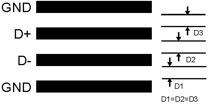
- Diode traces must be surrounded by a GND guard ring to either side, above and below if possible. This GND guard must not be between the D+ and D− lines. In the event that noise does couple to the diode lines it would be ideal if it is coupled common mode. That is equally to the D+ and D− lines.
- Avoid routing diode traces in close proximity to power supply switching or filtering inductors.
- Avoid running diode traces close to or parallel to high-speed digital and bus lines. Diode traces must be kept at least 2 cm apart from the high-speed digital traces.
- If it is necessary to cross high-speed digital traces, the diode traces and the high-speed digital traces must cross at a 90 degree angle.
- The ideal place to connect the LM95214's GND pin is as close as possible to the Processors GND associated with the sense diode.
- Leakage current between D+ and GND and between D+ and D− must be kept to a minimum. Thirteen nano-amperes of leakage can cause as much as 0.2°C of error in the diode temperature reading. Keeping the printed-circuit board as clean as possible will minimize leakage current.
Noise coupling into the digital lines greater than 400 mVp-p (typical hysteresis) and undershoot less than 500 mV below GND, may prevent successful SMBus communication with the LM95214. SMBus no acknowledge is the most common symptom, causing unnecessary traffic on the bus. Although the SMBus maximum frequency of communication is rather low (100 kHz maximum), care still needs to be taken to ensure proper termination within a system with multiple parts on the bus and long printed-circuit board traces. An RC lowpass filter with a 3-dB corner frequency of about 40 MHz is included on the LM95214's SMBCLK input. Additional resistance can be added in series with the SMBDAT and SMBCLK lines to further help filter noise and ringing. Minimize noise coupling by keeping digital traces out of switching power supply areas as well as ensuring that digital lines containing high-speed data communications cross at right angles to the SMBDAT and SMBCLK lines.
10.2 Layout Example
 Figure 27. Ideal Diode Trace Layout