SNIS146B March 2007 – October 2017 LM95214
PRODUCTION DATA.
- 1 Features
- 2 Applications
- 3 Description
- 4 Revision History
- 5 Pin Configuration and Functions
-
6 Specifications
- 6.1 Absolute Maximum Ratings
- 6.2 ESD Ratings
- 6.3 Recommended Operating Conditions
- 6.4 Thermal Information
- 6.5 Electrical Characteristics: Temperature-to-Digital Converter
- 6.6 Logic Electrical Characteristics: Digital DC Characteristics
- 6.7 Switching Characteristics: SMBus Digital
- 6.8 Typical Characteristics
-
7 Detailed Description
- 7.1 Overview
- 7.2 Functional Block Diagram
- 7.3 Feature Description
- 7.4 Device Functional Modes
- 7.5 Register Maps
- 8 Application and Implementation
- 9 Power Supply Recommendations
- 10Layout
- 11Device and Documentation Support
- 12Mechanical, Packaging, and Orderable Information
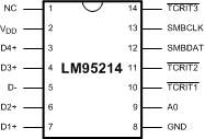
5 Pin Configuration and Functions
NHL Package
14-Pin WSON
Top View

Pin Functions
| PIN | DESCRIPTION | ||
|---|---|---|---|
| NO. | NAME | ||
| 1 | NC | No Connect Not connected. May be left floating, connected to GND or VDD. |
|
| 2 | VDD | Positive Supply Voltage Input DC Voltage from 3.0 V to 3.6 V. VDD must be bypassed with a 0.1-µF capacitor in parallel with 100 pF. The 100-pF capacitor must be placed as close as possible to the power supply pin. Noise must be kept below 200 mVp-p, a 10-µF capacitor may be required to achieve this. |
|
| 3 | D4+ | Diode Current Source Fourth Diode Anode. Connected to remote discrete diode-connected transistor junction or to the diode-connected transistor junction on a remote IC whose die temperature is being sensed. A capacitor is not required between D4+ and D–. A 100 pF capacitor between D4+ and D– can be added and may improve performance in noisy systems. Float this pin if this thermal diode is not used. |
|
| 4 | D3+ | Diode Current Source Third Diode Anode. Connected to remote discrete diode-connected transistor junction or to the diode-connected transistor junction on a remote IC whose die temperature is being sensed. A capacitor is not required between D3+ and D–. A 100-pF capacitor between D3+ and D– can be added and may improve performance in noisy systems. Float this pin if this thermal diode is not used. |
|
| 5 | D− | Diode Return Current Sink All Diode Cathodes. Common D– pin for all four remote diodes. |
|
| 6 | D2+ | Diode Current Source Second Diode Anode. Connected to remote discrete diode-connected transistor junction or to the diode-connected transistor junction on a remote IC whose die temperature is being sensed. A capacitor is not required between D2+ and D–. A 100-pF capacitor between D2+ and D– can be added and may improve performance in noisy systems. Float this pin if this thermal diode is not used. |
|
| 7 | D1+ | Diode Current Source First Diode Anode. Connected to remote discrete diode-connected transistor junction or to the diode-connected transistor junction on a remote IC whose die temperature is being sensed. A capacitor is not required between D1+ and D–. A 100-pF capacitor between D1+ and D– can be added and may improve performance in noisy systems. Float this pin if this thermal diode is not used. |
|
| 8 | GND | Power Supply Ground -- System low noise ground. | |
| 9 | A0 | Digital Input SMBus slave address select pin. Selects one of three addresses. Can be tied to VDD, GND, or to the middle of a resistor divider connected between VDD and GND. |
|
| 10 | TCRIT1 | Digital Output, Open-Drain Critical temperature output 1. Requires pullup resistor. Active LOW. |
|
| 11 | TCRIT2 | Digital Output, Open-Drain Critical temperature output 2. Requires pullup resistor. Active LOW. |
|
| 12 | SMBDAT | SMBus Bidirectional Data Line, Open-Drain Output From and to Controller; may require an external pullup resistor |
|
| 13 | SMBCLK | SMBus Clock Input From Controller; may require an external pullup resistor |
|
| 14 | TCRIT3 | Digital Output, Open-Drain Critical temperature output 3. Requires pullup resistor. Active LOW. |
|
Table 1. ESD Protection
| PIN NO. | LABEL | CIRCUIT | CIRCUITS FOR PIN ESD PROTECTION STRUCTURE |
|---|---|---|---|
| 1 | NC | – |  |
| 2 | VDD | A | |
| 3 | D4+ | A | |
| 4 | D3+ | A | |
| 5 | D- | A | |
| 6 | D2+ | A | |
| 7 | D1+ | A | Circuit A |
| 8 | GND | – |  |
| 9 | A0 | B | |
| 10 | TCRIT1 | B | |
| 11 | TCRIT2 | B | |
| 12 | SMBDAT | B | |
| 13 | SMBCLK | B | |
| 14 | TCRIT2 | B | Circuit B |