ZHCSIZ1G May 2010 – November 2018 LM98640QML-SP
PRODUCTION DATA.
- 1 特性
- 2 应用
- 3 说明
- 4 修订历史记录
- 5 Pin Configuration and Functions
- 6 Specifications
-
7 Detailed Description
- 7.1 Overview
- 7.2 Functional Block Diagram
- 7.3 Feature Description
- 7.4
Device Functional Mode
- 7.4.1 Powerdown Modes
- 7.4.2
LVDS Test Modes
- 7.4.2.1 Test Mode 0 - Fixed Pattern
- 7.4.2.2 Test Mode 1 - Horizontal Gradient
- 7.4.2.3 Test Mode 2 - Vertical Gradient
- 7.4.2.4 Test Mode 3 - Lattice Pattern
- 7.4.2.5 Test Mode 4 - Stripe Pattern
- 7.4.2.6 Test Mode 5 - LVDS Test Pattern (Synchronous)
- 7.4.2.7 Test Mode 6 - LVDS Test Pattern (Asynchronous)
- 7.4.2.8 Pseudo Random Number Mode
- 7.5 Programming
- 7.6 Register Maps
- 8 Application and Implementation
- 9 Layout
- 10器件和文档支持
- 11机械、封装和可订购信息
7.3.1.1.1 Sample & Hold Mode CLAMP/SAMPLE Adjust
For accurate sampling of the input signals the LM98640QML-SP allows for full adjustment of the internal SAMPLE pulse to align it to the proper positions over the input signal. In Sample & Hold mode the SAMPLE pulse should be placed over the pixel output period of the image sensor. Only the Sample Start and Sample End Registers (0x22,0x23) need to be configured, the Clamp Start and Clamp End Registers (0x20,0x21) are not valid in Sample & Hold Mode. Internally the input clock is divided into 64 edges per clock period, the Sample Start and Sample End Registers correspond to the internal edge number the SAMPLE pulse will start and end. To adjust the SAMPLE pulse, first send the CLAMP and SAMPLE signals to the DTM pins by writing 10 to bits[4:3] of the Clock Monitor Register (0x09). This will allow the user to observe the SAMPLE pulse on pin DTM1 along with the image sensor output using an oscilloscope. Then, using the Sample Start and End Registers, adjust the SAMPLE pulse to align it over the Video Level portion of the image sensor output. To allow for settling and to reduce noise, the SAMPLE pulse should be made as wide as possible and fill the entire Video Level portion of the input signal.
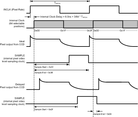
Figure 15 shows some examples of an input waveform and where the SAMPLE pulse should be placed. Ideally the image sensor output would line up directly with the input clock at the AFE inputs, but due to trace delays in the system the image sensor output is delayed relative to the input clock. In the delayed image sensor waveform the Sample Start value is higher than the Sample End value. In this situation the SAMPLE pulse will start in one clock period and wraps around to the next. This allows the LM98640QML-SP to adjust for the delay in the image sensor waveform. Notice that edge zero of the internal clock does not line up with the rising edge of the input clock. This is due to internal delays of the clock signals. The amount of delay can be calculated from operating frequency using the following formula: tDCLK = 6.0 ns + 3 / 64 × TINCLK
 Figure 15. S/H Mode CLAMP/SAMPLE Adjust