ZHCSIZ1G May 2010 – November 2018 LM98640QML-SP
PRODUCTION DATA.
- 1 特性
- 2 应用
- 3 说明
- 4 修订历史记录
- 5 Pin Configuration and Functions
- 6 Specifications
-
7 Detailed Description
- 7.1 Overview
- 7.2 Functional Block Diagram
- 7.3 Feature Description
- 7.4
Device Functional Mode
- 7.4.1 Powerdown Modes
- 7.4.2
LVDS Test Modes
- 7.4.2.1 Test Mode 0 - Fixed Pattern
- 7.4.2.2 Test Mode 1 - Horizontal Gradient
- 7.4.2.3 Test Mode 2 - Vertical Gradient
- 7.4.2.4 Test Mode 3 - Lattice Pattern
- 7.4.2.5 Test Mode 4 - Stripe Pattern
- 7.4.2.6 Test Mode 5 - LVDS Test Pattern (Synchronous)
- 7.4.2.7 Test Mode 6 - LVDS Test Pattern (Asynchronous)
- 7.4.2.8 Pseudo Random Number Mode
- 7.5 Programming
- 7.6 Register Maps
- 8 Application and Implementation
- 9 Layout
- 10器件和文档支持
- 11机械、封装和可订购信息
7.3.2.2 CDS Mode Biasing
Correlated Double Sampling mode does not require as precise a DC bias point as does Sample and Hold mode. This is due mainly to the nature of CDS itself, that is, the Video Signal voltage is referenced to the Reset Level voltage instead of the static DC VCLP voltage. The common mode voltage of these two points on the CCD waveform have little bearing on the resulting differential result. However, the DC bias point does need to be established to ensure the CCD waveform’s common mode voltage is within rated operating ranges.
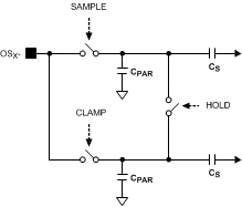
 Figure 21. CDS Mode Simplified Input Diagram
 The CDS mode biasing can be performed in the same way as described in the Sample and Hold Mode Biasing section, or, an external resistor divider can be placed across the OSX– input to provide the DC bias voltage. In CDS Mode the OSX+ pins should each be decoupled with 0.1-µF capacitors to ground.
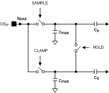
 Figure 22. CDS Mode Input Bias Current
 Unlike in Sample and Hold Mode, the input bias current in CDS Mode is relatively small. Due to the architecture of CDS switching, the average charge loss or gain on the input node is ideally zero over the duration of a pixel. This results in a much lower input bias current, whose main source is parasitic impedances and leakage currents. As a result of the lower input bias current in CDS Mode, maintaining the DC Bias point the input node over the length of a line will require a much smaller AC input coupling capacitor.