ZHCSUM4D November 1994 – February 2024 LMC6032 , LMC6034
PRODUCTION DATA
4 Pin Configuration and Functions
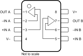
 LMC6032
D Package, 8-Pin SOIC, and P Package, 8-Pin PDIP (Top View)
LMC6032
D Package, 8-Pin SOIC, and P Package, 8-Pin PDIP (Top View)Table 4-1 Pin Functions: LMC6032
| PIN | TYPE | DESCRIPTION | |
|---|---|---|---|
| NAME | NO. | ||
| +IN A | 3 | Input | Noninverting input, channel A |
| –IN A | 2 | Input | Inverting input, channel A |
| +IN B | 5 | Input | Noninverting input, channel B |
| –IN B | 6 | Input | Inverting input, channel B |
| OUT A | 1 | Output | Output, channel A |
| OUT B | 7 | Output | Output, channel B |
| V+ | 8 | Power | Positive (highest) power supply |
| V– | 4 | Power | Negative (lowest) power supply |
 LMC6034
D Package, 14-Pin SOIC, and P Package, 14-Pin PDIP (Top View)
LMC6034
D Package, 14-Pin SOIC, and P Package, 14-Pin PDIP (Top View)Table 4-2 Pin Functions: LMC6034
| PIN | TYPE | DESCRIPTION | |
|---|---|---|---|
| NAME | NO. | ||
| +IN A | 3 | Input | Noninverting input, channel A |
| +IN B | 5 | Input | Noninverting input, channel B |
| +IN C | 10 | Input | Noninverting input, channel C |
| +IN D | 12 | Input | Noninverting input, channel D |
| –IN A | 2 | Input | Inverting input, channel A |
| –IN B | 6 | Input | Inverting input, channel B |
| –IN C | 9 | Input | Inverting input, channel C |
| –IN D | 13 | Input | Inverting input, channel D |
| OUT A | 1 | Output | Output, channel A |
| OUT B | 7 | Output | Output, channel B |
| OUT C | 8 | Output | Output, channel C |
| OUT D | 14 | Output | Output, channel D |
| V+ | 4 | Power | Positive (highest) power supply |
| V– | 11 | Power | Negative (lowest) power supply |