ZHCSTR2E August 2000 – February 2024 LMC6081 , LMC6082 , LMC6084
PRODUCTION DATA
6.1.2 Compensating for Input Capacitance
The use of large value feedback resistors is quite common for amplifiers with ultra-low input current, like the LMC608x.
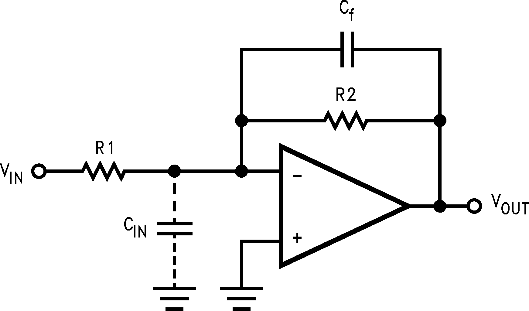
Although the LMC608x are highly stable over a wide range of operating conditions, certain precautions must be met to achieve the desired pulse response when a large feedback resistor is used. Large feedback resistors and even small values of input capacitance, due to transducers, photodiodes, and circuit board parasitics, reduce phase margins.
When a high input impedance is demanded, guarding of the LMC608x is suggested. Guarding input lines not only reduces leakage, but lowers stray input capacitance as well. (See Printed-Circuit-Board Layout for High Impedance Work)
The effect of input capacitance can be compensated for by adding a capacitor, Cf, around the feedback resistors (as in Figure 6-1 ) such that:
or
The exact value of CIN can be difficult to find, so Cf can be experimentally adjusted so that the desired pulse response is achieved. Refer to the LMC66x for a more detailed discussion on compensating for input capacitance.
 Figure 6-1 Canceling the Effect of Input
Capacitance