SNOS753F August 1999 – January 2025 LMC7111
PRODUCTION DATA
- 1
- 1 Features
- 2 Applications
- 3 Description
- 4 Pin Configuration and Functions
-
5 Specifications
- 5.1 Absolute Maximum Ratings
- 5.2 ESD Ratings
- 5.3 Recommended Operating Conditions
- 5.4 Thermal Information
- 5.5 Electrical Characteristics for VS = 2.7V or ±1.35V
- 5.6 Electrical Characteristics for VS = 5V or ±2.5V
- 5.7 Electrical Characteristics for VS = 10V or ±5V
- 5.8 Typical Characteristics
- 5.9 Typical Characteristics: 2.7V
- 5.10 Typical Characteristics: 3V
- 5.11 Typical Characteristics: 5V
- 5.12 Typical Characteristics: 10V
- 6 Detailed Description
- 7 Application and Implementation
- 8 Device and Documentation Support
- 9 Revision History
- 10Mechanical, Packaging, and Orderable Information
7.1.1 Capacitive Load Tolerance
The LMC7111 can typically directly drive a 300pF load with VS = 10V at unity gain without oscillating. The unity gain follower is the most sensitive configuration. Direct capacitive loading reduces the phase margin of op-amps. The combination of the op-amp output impedance and the capacitive load induces phase lag. This results in either an underdamped pulse response or oscillation.
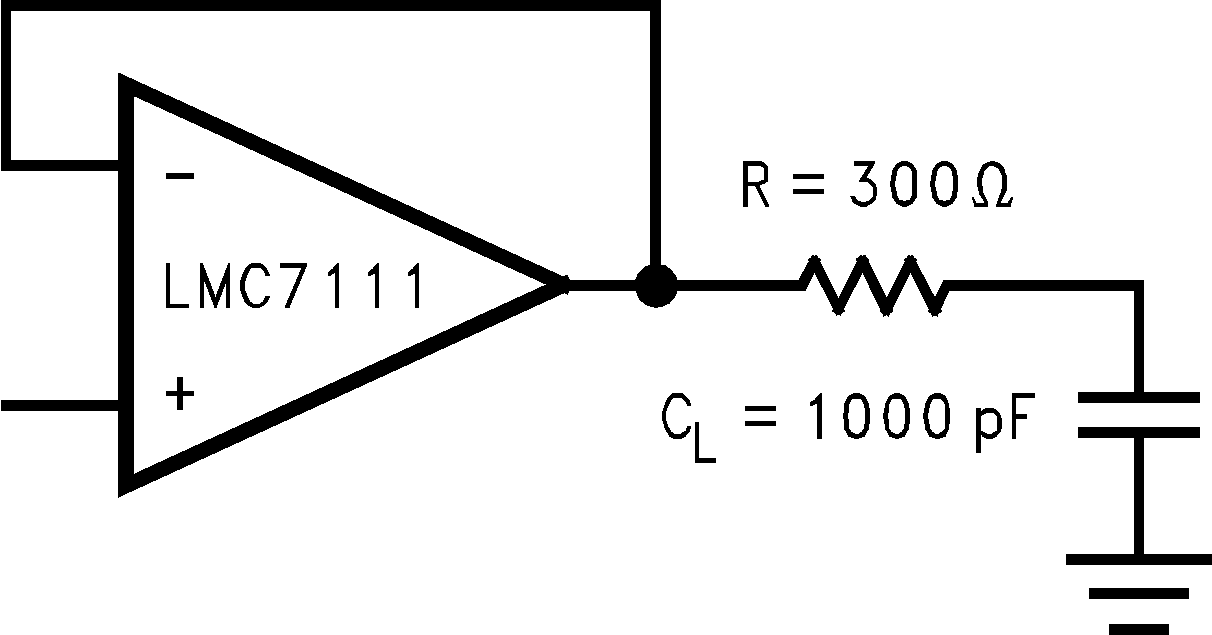
Capacitive load compensation can be accomplished using resistive isolation as shown in Figure 7-1. This simple technique is useful for isolating the capacitive input of multiplexers and A/D converters.
 Figure 7-1 Resistive Isolation
of a 330pF Capacitive Load