ZHCSHN8B February   2018  – October 2018 LMG1020

PRODUCTION DATA.  

  1. 特性
  2. 应用
  3. 说明
    1.     Device Images
      1.      简化的激光雷达 (LiDAR) 驱动器级图
  4. 修订历史记录
  5. Pin Configuration and Functions
    1.     Pin Functions
  6. Specifications
    1. 6.1 Absolute Maximum Ratings
    2. 6.2 ESD Ratings
    3. 6.3 Recommended Operating Conditions
    4. 6.4 Thermal Information
    5. 6.5 Electrical Characteristics
    6. 6.6 Switching Characteristics
    7. 6.7 Typical Characteristics
  7. Detailed Description
    1. 7.1 Overview
    2. 7.2 Functional Block Diagram
    3. 7.3 Feature Description
      1. 7.3.1 Input Stage
      2. 7.3.2 Output Stage
      3. 7.3.3 VDD and undervoltage lockout
      4. 7.3.4 Overtemperature Protection (OTP)
    4. 7.4 Device Functional Modes
  8. Application and Implementation
    1. 8.1 Application Information
    2. 8.2 Typical Application
      1. 8.2.1 Design Requirements
      2. 8.2.2 Detailed Design Procedure
        1. 8.2.2.1 Handling Ground Bounce
        2. 8.2.2.2 Creating Nanosecond Pulse With LMG1020
      3. 8.2.3 VDD and Overshoot
      4. 8.2.4 Operating at Higher Frequency
      5. 8.2.5 Application Curves
  9. Power Supply Recommendations
  10. 10Layout
    1. 10.1 Layout Guidelines
      1. 10.1.1 Gate Drive Loop Inductance and Ground Connection
      2. 10.1.2 Bypass Capacitor
    2. 10.2 Layout Example
  11. 11器件和文档支持
    1. 11.1 文档支持
      1. 11.1.1 相关文档
    2. 11.2 接收文档更新通知
    3. 11.3 社区资源
    4. 11.4 商标
    5. 11.5 静电放电警告
    6. 11.6 术语表
  12. 12机械、封装和可订购信息

封装选项

机械数据 (封装 | 引脚)
散热焊盘机械数据 (封装 | 引脚)
订购信息

Typical Application

The LMG1020 is designed to be used with a single low-side, ground-referenced GaN or logic-level Si FET, as shown in Figure 6. Independent gate drive resistors, R1 and R2, are used to independently control the turnon and turnoff drive strengths, respectively. For fast and strong turnoff, R2 can be shorted and OUTL directly connected to the transistor’s gate. For symmetric drive strengths, it is acceptable to short OUTH and OUTL and use a single gate-drive resistor.

TI recommends using at least a 2 Ω resistor at each OUTH and OUTL to avoid voltage overstress due to inductive ringing. Ringing overshoot must not exceed the maximum absolute supply voltage.

For applications requiring smaller resistance values, contact TI E2E for guidance.
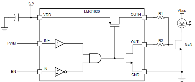
LMG1020 bearcat-system-diagram.gifFigure 6. Typical Implementation of a Circuit