ZHCSHN8B February 2018 – October 2018 LMG1020
PRODUCTION DATA.
8.2.5 Application Curves
 Figure 11. 90 ns Pulse from Function Generator Yielding 15 ns Pulse On The Input (Cyan) And Gate (Blue) After Pulse Shortening
  Figure 13. 1.2 ns Gate Pulse Yielding 1.5 ns 30V Into 1 Ω Pulse (500MHz Scope)
  Figure 12. 90 ns Pulse from Function Generator Yielding 1.5 ns Pulse On The Input (Cyan) And Gate (Blue) After Pulse Shortening
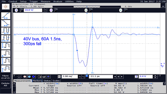
  Figure 14. VDS for 1.5 ns Pulse With 40V of Bus Voltage
 Figure 11 and Figure 12 are the waveforms showing the pulse short pulse generation and input/output pulses. The 90ns long pulse (in green color) and its delayed signal are sent through an AND gate, which outputs a short pulse signal as the input of LMG1020. The output signal (in blue color) follows the input (in cyan color) with certain propagation delay. An output pulse short as 1.5 ns can be obtained as Figure 12.
Figure 13 is taken with a 500MHz oscilloscope and shows typical operation waveforms, including the input logic gating signal (cyan), gate signal (blue), and drain to source signal (pink) of the switching GaN FET. On the drain waveform of the FET, it is possible to see a 20V overshoot. This is due to the inductance in the power loop. Vg seems to be oscillating, but this is caused by pickup noise, which is inevitable even when using a spring ground connection.
Figure 14 shows the waveform of drain to source voltage of a FET driven by LMG1020 with 1.5ns pulse width and 300ps fall time, which drives maximum 60A current at 40V bus voltage.