ZHCSHN8B February   2018  – October 2018 LMG1020

PRODUCTION DATA.  

  1. 特性
  2. 应用
  3. 说明
    1.     Device Images
      1.      简化的激光雷达 (LiDAR) 驱动器级图
  4. 修订历史记录
  5. Pin Configuration and Functions
    1.     Pin Functions
  6. Specifications
    1. 6.1 Absolute Maximum Ratings
    2. 6.2 ESD Ratings
    3. 6.3 Recommended Operating Conditions
    4. 6.4 Thermal Information
    5. 6.5 Electrical Characteristics
    6. 6.6 Switching Characteristics
    7. 6.7 Typical Characteristics
  7. Detailed Description
    1. 7.1 Overview
    2. 7.2 Functional Block Diagram
    3. 7.3 Feature Description
      1. 7.3.1 Input Stage
      2. 7.3.2 Output Stage
      3. 7.3.3 VDD and undervoltage lockout
      4. 7.3.4 Overtemperature Protection (OTP)
    4. 7.4 Device Functional Modes
  8. Application and Implementation
    1. 8.1 Application Information
    2. 8.2 Typical Application
      1. 8.2.1 Design Requirements
      2. 8.2.2 Detailed Design Procedure
        1. 8.2.2.1 Handling Ground Bounce
        2. 8.2.2.2 Creating Nanosecond Pulse With LMG1020
      3. 8.2.3 VDD and Overshoot
      4. 8.2.4 Operating at Higher Frequency
      5. 8.2.5 Application Curves
  9. Power Supply Recommendations
  10. 10Layout
    1. 10.1 Layout Guidelines
      1. 10.1.1 Gate Drive Loop Inductance and Ground Connection
      2. 10.1.2 Bypass Capacitor
    2. 10.2 Layout Example
  11. 11器件和文档支持
    1. 11.1 文档支持
      1. 11.1.1 相关文档
    2. 11.2 接收文档更新通知
    3. 11.3 社区资源
    4. 11.4 商标
    5. 11.5 静电放电警告
    6. 11.6 术语表
  12. 12机械、封装和可订购信息

封装选项

机械数据 (封装 | 引脚)
散热焊盘机械数据 (封装 | 引脚)
订购信息

Pin Configuration and Functions

YFF Package
6-Ball WCSP
Top View
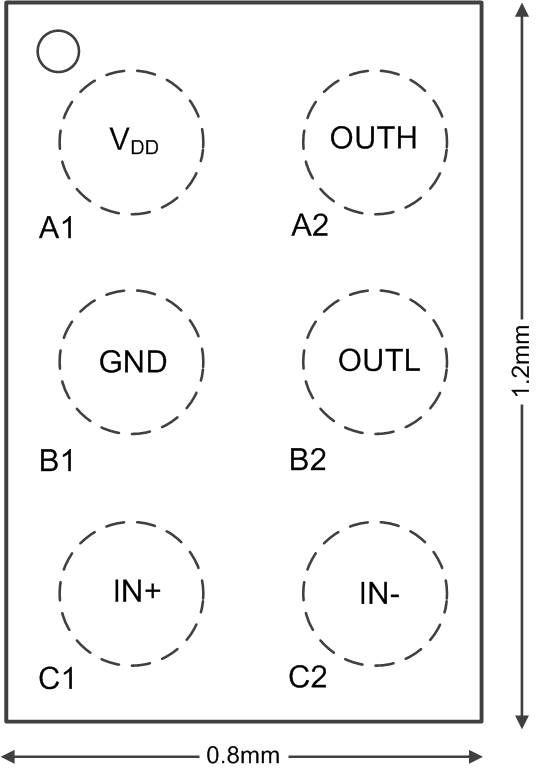
LMG1020 lmg1020-package-top-view-snosd45.gif

Pin Functions

PIN I/O DESCRIPTION
NAME NO.
GND B1 Ground
IN+ C1 I Positive logic-level input
IN– C2 I Negative logic-level input
OUTL B2 O Pulldown gate drive output. Connect through an optional resistor to the target transistor’s gate
OUTH A2 O Pullup gate drive output. Connect through a resistor to the target transistor’s gate
VDD A1 I Input voltage supply. Decouple through a small size, low inductance capacitor to GND