ZHCSG61B march 2017 – april 2023 LMG1205
PRODUCTION DATA
5 Pin Configuration and Functions
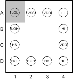
 Figure 5-1 YFX Package12-Pin DSBGATop View
Table 5-1 Pin Functions
| PIN | TYPE (2) | DESCRIPTION | |||
|---|---|---|---|---|---|
| NUMBER | NAME | ||||
| A1 | LOL | O | Low-side gate driver sink-current output: connect to the gate of the low-side GaN FET with a short, low inductance path. A gate resistor can be used to adjust the turnoff speed. | ||
| A2 | VSS | G | Ground return: all signals are referenced to this ground. | ||
| A3, C4(1) | VDD | P | 5-V positive gate drive supply: locally decouple to VSS using low ESR/ESL capacitor located as close as possible to the IC. | ||
| A4 | LI | I | Low-side driver control input. The LMG1205 inputs have TTL type thresholds. Unused inputs must be tied to ground and not left open. | ||
| B1 | LOH | O | Low-side gate driver source-current output: connect to the gate of low-side GaN FET with a short, low inductance path. A gate resistor can be used to adjust the turnon speed. | ||
| B4 | HI | I | High-side driver control input. The LMG1205 inputs have TTL type thresholds. Unused inputs must be tied to ground and not left open. | ||
| C1, D4(1) | HS | P | High-side GaN FET source connection: connect to the bootstrap capacitor negative terminal and the source of the high-side GaN FET. | ||
| D1 | HOL | O | High-side gate driver turnoff output: connect to the gate of high-side GaN FET with a short, low inductance path. A gate resistor can be used to adjust the turnoff speed. | ||
| D2 | HOH | O | High-side gate driver turnon output: connect to the gate of high-side GaN FET with a short, low inductance path. A gate resistor can be used to adjust the turnon speed. | ||
| D3 | HB | P | High-side gate driver bootstrap rail: connect the positive terminal of the bootstrap capacitor to HB and the negative terminal to HS. The bootstrap capacitor must be placed as close as possible to the IC. | ||
(1) A3 and C4, C1 and D4 are internally connected
(2) I = Input, O = Output, G = Ground, P = Power