ZHCSHO1D November 2018 – January 2019 LMG1210
PRODUCTION DATA.
7.3.6 Negative HS Voltage Handling
The LMG1210 by itself can operate with -200V on the HS pin as stated in the recommended operating conditions table. However, if using a bootstrap diode, the system will be more limited based on the potential of high-currents flowing through the bootstrap diode.
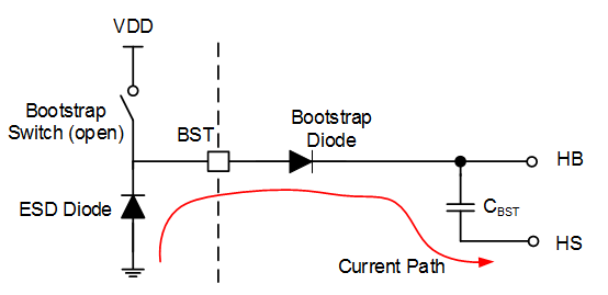
HS goes most negative during the dead times when the low-side FET is off. This also means the bootstrap switch is off so the BST pin is relatively high impedance. Therefore as HS goes negative, the bootstrap diode becomes forward biased and pulls the voltage at BST down with it. Because the bootstrap switch is off, very little current will flow until the bootstrap diode attempts to pull the BST pin below ground at which point the ESD diode on the BST pin will clamp the voltage at a diode drop below ground. The point where significant current begins to flow through the bootstrap diode is given in Equation 6
Where VBST is the forward voltage drop of the selected bootstrap diode and VESD is the forward voltage drop of the ESD diode of the BST pin which is typically 0.7V at room temp. Figure 15 shows a schematic of this current path.
 Figure 15. Current Path Across Bootstrap Diode
 Once this negative voltage is exceeded, large currents will begin to flow out of the BST pin and through the bootstrap diode. The currents may be limited by the following: resistance of the BST ESD diode, resistance of the bootstrap diode, inductance of the bootstrap loop, or additional resistance purposely added in series with the bootstrap diode. If this current is too high, damage to the bootstrap diode or the LMG1210 can result. If this current delivers significant enough total charge, this can over-charge the bootstrap rail as well.
The BST pin ESD diode has been specifically designed to be robust to carry up to a couple amps surge current without damage.