ZHCSHO1D November   2018  – January 2019 LMG1210

PRODUCTION DATA.  

  1. 特性
  2. 应用
  3. 说明
    1.     Device Images
      1.      简化的典型应用
  4. 修订历史记录
  5. Pin Configuration and Functions
    1.     Pin Functions
  6. Specifications
    1. 6.1 Absolute Maximum Ratings
    2. 6.2 ESD Ratings
    3. 6.3 Recommended Operating Conditions
    4. 6.4 Thermal Information
    5. 6.5 Electrical Characteristics
    6. 6.6 Switching Characteristics
    7. 6.7 Typical Characteristics
    8. 6.8 Timing Diagrams
  7. Detailed Description
    1. 7.1 Overview
    2. 7.2 Functional Block Diagram
    3. 7.3 Feature Description
      1. 7.3.1 Bootstrap Diode Operation
      2. 7.3.2 LDO Operation
      3. 7.3.3 Dead Time Selection
      4. 7.3.4 Overtemperature Protection
      5. 7.3.5 High-Performance Level Shifter
      6. 7.3.6 Negative HS Voltage Handling
    4. 7.4 Device Functional Modes
  8. Application and Implementation
    1. 8.1 Application Information
    2. 8.2 Typical Application
      1. 8.2.1 Design Requirements
      2. 8.2.2 Detailed Design Procedure
        1. 8.2.2.1 Bypass Capacitor
        2. 8.2.2.2 Bootstrap Diode Selection
        3. 8.2.2.3 Handling Ground Bounce
        4. 8.2.2.4 Independent Input Mode
        5. 8.2.2.5 Computing Power Dissipation
      3. 8.2.3 Application Curves
    3. 8.3 Do's and Don'ts
  9. Power Supply Recommendations
  10. 10Layout
    1. 10.1 Layout Guidelines
    2. 10.2 Layout Example
  11. 11器件和文档支持
    1. 11.1 文档支持
      1. 11.1.1 相关文档
    2. 11.2 接收文档更新通知
    3. 11.3 社区资源
    4. 11.4 商标
    5. 11.5 静电放电警告
    6. 11.6 术语表
  12. 12机械、封装和可订购信息

封装选项

机械数据 (封装 | 引脚)
  • RVR|19
散热焊盘机械数据 (封装 | 引脚)
订购信息

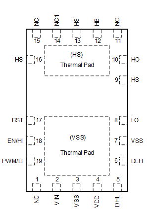
Pin Configuration and Functions

RVR Package
19-Pin WQFN
Top View
LMG1210 pin_diagram_snosd12.gif

Pin Functions

PIN I/O DESCRIPTION
NAME NO.
BST 17 O Bootstrap diode anode connection point.
DHL 5 I Sets the dead time for a high-to-low transition in PWM mode by connecting a resistor to VSS. If using IIM this pin can be left floating, tied to GND, tied to VDD.
DLH 6 I Sets the dead time for a low-to-high transition in PWM mode by connecting a resistor to VSS. Tie to VDD to select IIM.
EN/HI 18 I Enable input or high-side driver control. In PWM mode this is the EN pin. In IIM mode this is the HI pin.
PWM/LI 19 I PWM input or low-side driver control. In PWM mode this is the PWM pin. In IIM mode this is the LI pin.
HB 12 I High-side driver supply. Bootstrap diode cathode connection point.
HO 10 O High-side driver output.
HS 9,13,16 I Switch node and high-side driver ground. These pins are internally connected.
LO 8 O Low-side driver output.
NC 1,11,15 Not internally connected.
NC1 14 I For proper operation, this pin should be either unconnected or tied to HS.
Thermal Pad (HS) 21 I Connected to HS.
Thermal Pad (VSS) 20 I Connected to VSS.
VDD 4 O Low-side driver supply and LDO output. 5 V
VIN 2 I 6 V to 18 V input to LDO. If LDO is not required, connect to VDD.
VSS 3,7 Low-side ground return: all low-side signals are referenced to this ground.