ZHCSIP2E April   2016  – October 2018 LMG3410R070 , LMG3411R070

PRODUCTION DATA.  

  1. 特性
  2. 应用
  3. 说明
    1.     Device Images
      1.      简化方框图
      2.      高于 100V/ns 时的开关性能
  4. 修订历史记录
  5. Pin Configuration and Functions
    1.     Pin Functions
  6. Specifications
    1. 6.1 Absolute Maximum Ratings
    2. 6.2 ESD Ratings
    3. 6.3 Recommended Operating Conditions
    4. 6.4 Thermal Information
    5. 6.5 Electrical Characteristics
    6. 6.6 Switching Characteristics
    7. 6.7 Typical Characteristics
  7. Parameter Measurement Information
    1. 7.1 Switching Parameters
      1. 7.1.1 Turn-on Delays
      2. 7.1.2 Turn-off Delays
      3. 7.1.3 Drain Slew Rate
      4. 7.1.4 Turn-on and Turn-off Energy
  8. Detailed Description
    1. 8.1 Overview
    2. 8.2 Functional Block Diagram
    3. 8.3 Feature Description
      1. 8.3.1 Direct-Drive GaN Architecture
      2. 8.3.2 Internal Buck-Boost DC-DC Converter
      3. 8.3.3 Internal Auxiliary LDO
      4. 8.3.4 Fault Detection
        1. 8.3.4.1 Over-current Protection
        2. 8.3.4.2 Over-Temperature Protection and UVLO
      5. 8.3.5 Drive Strength Adjustment
    4. 8.4 Device Functional Modes
      1. 8.4.1 Low-Power Mode
  9. Application and Implementation
    1. 9.1 Application Information
    2. 9.2 Typical Application
      1. 9.2.1 Design Requirements
      2. 9.2.2 Detailed Design Procedure
        1. 9.2.2.1 Slew Rate Selection
          1. 9.2.2.1.1 Startup and Slew Rate with Bootstrap High-Side Supply
        2. 9.2.2.2 Signal Level-Shifting
        3. 9.2.2.3 Buck-Boost Converter Design
      3. 9.2.3 Application Curves
    3. 9.3 Paralleling GaN Devices
    4. 9.4 Do's and Don'ts
  10. 10Power Supply Recommendations
    1. 10.1 Using an Isolated Power Supply
    2. 10.2 Using a Bootstrap Diode
      1. 10.2.1 Diode Selection
      2. 10.2.2 Managing the Bootstrap Voltage
      3. 10.2.3 Reliable Bootstrap Start-up
  11. 11Layout
    1. 11.1 Layout Guidelines
      1. 11.1.1 Power Loop Inductance
      2. 11.1.2 Signal Ground Connection
      3. 11.1.3 Bypass Capacitors
      4. 11.1.4 Switch-Node Capacitance
      5. 11.1.5 Signal Integrity
      6. 11.1.6 High-Voltage Spacing
      7. 11.1.7 Thermal Recommendations
    2. 11.2 Layout Example
  12. 12器件和文档支持
    1. 12.1 器件支持
      1. 12.1.1 第三方米6体育平台手机版_好二三四免责声明
    2. 12.2 文档支持
      1. 12.2.1 相关文档
    3. 12.3 接收文档更新通知
    4. 12.4 社区资源
    5. 12.5 商标
    6. 12.6 静电放电警告
    7. 12.7 术语表
  13. 13机械、封装和可订购信息

封装选项

机械数据 (封装 | 引脚)
散热焊盘机械数据 (封装 | 引脚)
订购信息

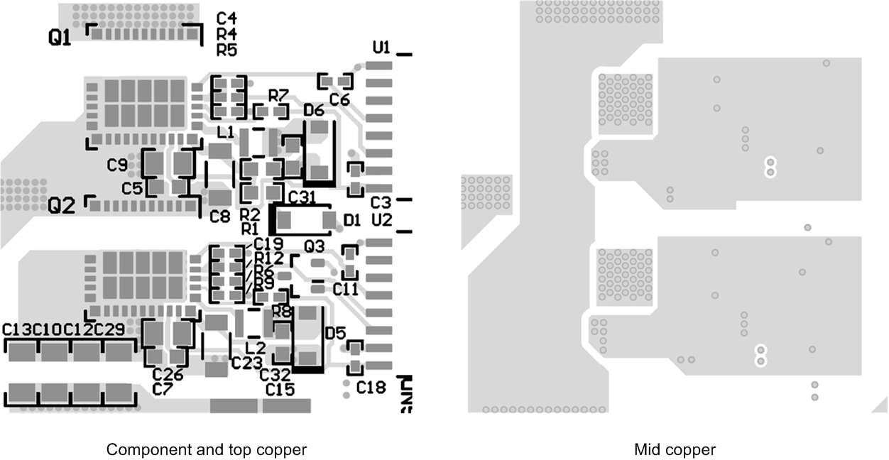
Layout Example

Correct layout of the LMG341xR070 and its surrounding components is essential for correct operation. The layout shown here reflects the power stage schematic in Figure 14. It may be possible to obtain acceptable performance with alternate layout schemes, however this layout has been shown to produce good results and is intended as a guideline.
LMG3410R070 LMG3411R070 ex_layout_snosd10.pngFigure 19. Example Half-Bridge Layout