ZHCSJF9A March 2019 – June 2019 LMG3410R150 , LMG3411R150
ADVANCE INFORMATION for pre-production products; subject to change without notice.
- 1 特性
- 2 应用
- 3 说明
- 4 修订历史记录
- 5 Pin Configuration and Functions
- 6 Specifications
- 7 Parameter Measurement Information
- 8 Detailed Description
- 9 Application and Implementation
- 10Power Supply Recommendations
- 11Layout
- 12器件和文档支持
- 13机械、封装和可订购信息
7 Parameter Measurement Information
Switching Parameters
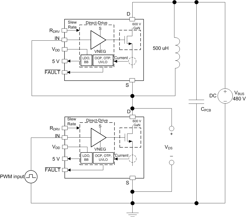
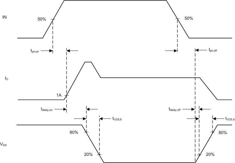
The circuit used to measure most switching parameters is shown in Figure 1. The top LMG341xR150 in this circuit is used to re-circulate the inductor current and functions in third-quadrant mode only. The bottom device is the active device; it is turned on to increase the inductor current to the desired test current. The bottom device is then turned off and on to create switching waveforms at a specific inductor current. Both the drain current (at the source) and the drain-source voltage is measured. The specific timing measurement is shown in Figure 2. It is recommended to use the half-bridge as double pulse tester. Excessive 3rd quadrant operation may over heat the top LMG341xR150.
 Figure 1. Circuit Used to Determine Switching Parameters
  Figure 2. Measurement to Determine Propagation Delays and Slew Rates
 Turn-on Delays
The timing of the turn-on transition has three components: propagation delay, turn-on delay and fall time. The first component is the propagation delay of the driver from when the input goes high to when the GaN FET starts turning on (represented by 1 A drain current). The turn-on delay is the delay from when the FET starts turning on to when the drain voltage swings down by 20 percent. Finally, the VDS fall time is the time it takes the drain voltage to slew between 80 percent and 20 percent of the bus voltage. The drive-strength resistor value has a large effect on turn-on delay and VDS fall time but does not affect the propagation delay significantly.
Turn-off Delays
The timing of the turn-off transition has three components: propagation delay, turn-off delay and rise time. The first component is the propagation delay of the driver from when the input goes low to when the GaN FET starts turning off. The turn-off delay is the delay from when the FET starts turning of (represented by the drain rising above 10 V) to when the drain voltage swings up by 20 percent. Finally, the VDS rise time is the time it takes the drain voltage to slew between 20 percent and 80 percent of the bus voltage. The turn-off delays of the LMG341xR150 are independent of the drive-strength resistor but the turn-off delay and the VDS rise time are heavily dependent on the load current.
Drain Slew Rate
The slew rate, measured in volts per nanosecond, is measured on the turn-on edge of the LMG341xR150. The slew rate is considered over the VDS fall time, where the drain falls from 80 percent to 20 percent of the bus voltage. The drain slew rate is thus given by 60 percent of the bus voltage divided by the VDS fall time. This drain slew rate is dependent on the RDRV value and is only slightly affected by drain current.