ZHCSIU1A September 2018 – March 2019 LMG3410R050 , LMG3411R050
ADVANCE INFORMATION for pre-production products; subject to change without notice.
- 1 特性
- 2 应用
- 3 说明
- 4 修订历史记录
- 5 Pin Configuration and Functions
- 6 Specifications
- 7 Parameter Measurement Information
- 8 Detailed Description
- 9 Application and Implementation
- 10Power Supply Recommendations
- 11Layout
- 12器件和文档支持
- 13机械、封装和可订购信息
8.3.4.1 Over-current Protection
The OCP circuit monitors the LMG341xR050's drain current and compares that current signal with an internally set limit. Upon detection of the over-current, the family of GaN FETs has two optional protection actions: 1) latched overcurrent protection; and 2) cycle-by-cycle overcurrent protection.
LMG3410R050 provides latched OCP option, by which the FET is shut off and held off until the fault is reset by either holding the IN pin low for more than 350 microseconds or removing power from VDD.
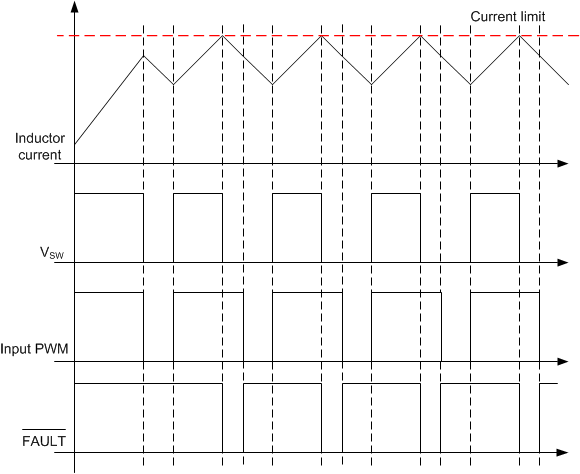
LMG3411R050 provides cycle-by-cycle OCP option. In this mode, the FET is also shut off when overcurrent happens, but the output fault signal will clear after the input PWM goes low. In the next cycle, the FET can turn on as normal. The cycle-by-cycle function can be used in cases where steady state operation current is below the OCP level but transient response can still reach high current, while the circuit operation cannot be paused. It also prevents the power stage from overheating by having overcurrent induced conduction loss.
During cycle-by-cycle operation, after the current reaches the upper limit but the PWM input is still high, the load current can flow through the third quadrant of the other FET of a half-bridge with no synchronous rectification. The extra high negative voltage drop (–6V to –8V) from drain to source could lead to high third quadrant loss, similar to dead time loss but with much longer time. An operation scheme of cycle-by-cycle current limitation is shown as Figure 3. Therefore, it is critical to design the control scheme to make sure the number of switching cycles in cycle-by-cycle mode is limited, or to change PWM input based on the fault signal to shorten the time in third quadrant conduction mode of the power stage.
OCP circuit has a 20ns typical blanking time at slew rate of 100V/ns to prevent false triggering during switch node transitions. The blanking time increases with respect to lower slew rates accordingly since lower slew rates results in longer switching transition time. This fast response OCP circuit protects the GaN device even under a hard short-circuit condition.
 Figure 3. Cycle-by-cycle OCP Operation