SNOSDI2 March   2024 LMG3425R050

PRODUCTION DATA  

  1.   1
  2. Features
  3. Applications
  4. Description
  5. Pin Configuration and Functions
  6. Specifications
    1. 5.1 Absolute Maximum Ratings
    2. 5.2 ESD Ratings
    3. 5.3 Recommended Operating Conditions
    4. 5.4 Thermal Information
    5. 5.5 Electrical Characteristics
    6. 5.6 Switching Characteristics
    7. 5.7 Typical Characteristics
  7. Parameter Measurement Information
    1. 6.1 Switching Parameters
      1. 6.1.1 Turn-On Times
      2. 6.1.2 Turn-Off Times
      3. 6.1.3 Drain-Source Turn-On Slew Rate
      4. 6.1.4 Turn-On and Turn-Off Switching Energy
    2. 6.2 Safe Operation Area (SOA)
      1. 6.2.1 Repetitive SOA
  8. Detailed Description
    1. 7.1 Overview
    2. 7.2 Functional Block Diagram
    3. 7.3 Feature Description
      1. 7.3.1  GaN FET Operation Definitions
      2. 7.3.2  Direct-Drive GaN Architecture
      3. 7.3.3  Drain-Source Voltage Capability
      4. 7.3.4  Internal Buck-Boost DC-DC Converter
      5. 7.3.5  VDD Bias Supply
      6. 7.3.6  Auxiliary LDO
      7. 7.3.7  Fault Protection
        1. 7.3.7.1 Overcurrent Protection and Short-Circuit Protection
        2. 7.3.7.2 Overtemperature Shutdown Protection
        3. 7.3.7.3 UVLO Protection
        4. 7.3.7.4 High-Impedance RDRV Pin Protection
        5. 7.3.7.5 Fault Reporting
      8. 7.3.8  Drive-Strength Adjustment
      9. 7.3.9  Temperature-Sensing Output
      10. 7.3.10 Ideal-Diode Mode Operation
        1. 7.3.10.1 Operational Ideal-Diode Mode
        2. 7.3.10.2 Overtemperature-Shutdown Ideal-Diode Mode
    4. 7.4 Start-Up Sequence
    5. 7.5 Device Functional Modes
  9. Application and Implementation
    1. 8.1 Application Information
    2. 8.2 Typical Application
      1. 8.2.1 Design Requirements
      2. 8.2.2 Detailed Design Procedure
        1. 8.2.2.1 Slew Rate Selection
        2. 8.2.2.2 Signal Level-Shifting
        3. 8.2.2.3 Buck-Boost Converter Design
      3. 8.2.3 Application Curves
    3. 8.3 Do's and Don'ts
    4. 8.4 Power Supply Recommendations
      1. 8.4.1 Using an Isolated Power Supply
      2. 8.4.2 Using a Bootstrap Diode
        1. 8.4.2.1 Diode Selection
        2. 8.4.2.2 Managing the Bootstrap Voltage
    5. 8.5 Layout
      1. 8.5.1 Layout Guidelines
        1. 8.5.1.1 Solder-Joint Reliability
        2. 8.5.1.2 Power-Loop Inductance
        3. 8.5.1.3 Signal-Ground Connection
        4. 8.5.1.4 Bypass Capacitors
        5. 8.5.1.5 Switch-Node Capacitance
        6. 8.5.1.6 Signal Integrity
        7. 8.5.1.7 High-Voltage Spacing
        8. 8.5.1.8 Thermal Recommendations
      2. 8.5.2 Layout Examples
  10. Device and Documentation Support
    1. 9.1 Documentation Support
      1. 9.1.1 Related Documentation
    2. 9.2 Receiving Notification of Documentation Updates
    3. 9.3 Support Resources
    4. 9.4 Trademarks
    5. 9.5 Electrostatic Discharge Caution
    6. 9.6 Export Control Notice
    7. 9.7 Glossary
  11. 10Revision History
  12. 11Mechanical, Packaging, and Orderable Information

封装选项

机械数据 (封装 | 引脚)
  • RQZ|54
散热焊盘机械数据 (封装 | 引脚)
订购信息

Mechanical, Packaging, and Orderable Information

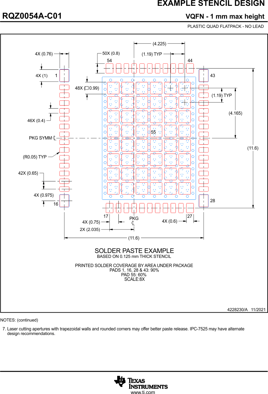
The following pages include mechanical, packaging, and orderable information. This information is the most current data available for the designated devices. This data is subject to change without notice and revision of this document. For browser-based versions of this data sheet, refer to the left-hand navigation.
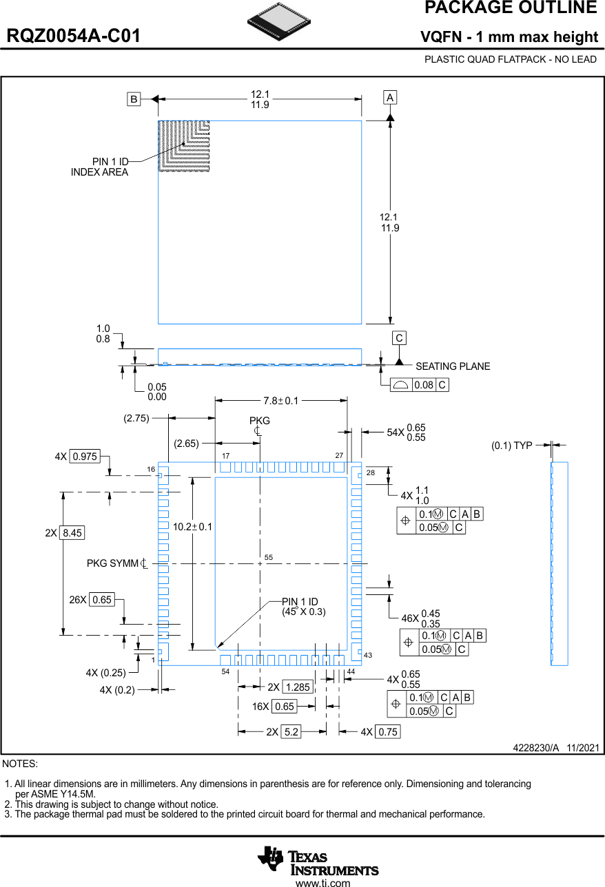
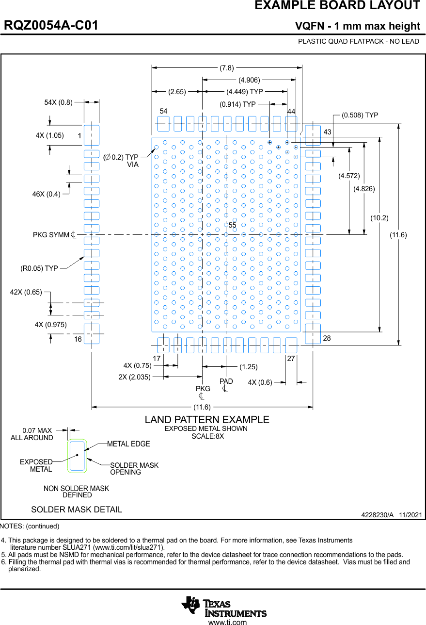
GUID-20211117-SS0I-FLQJ-7Q68-G4BMH4LK90CB-low.gif
GUID-20211117-SS0I-ZV9B-X7XX-WLMSFZFZD79T-low.gif
GUID-20211117-SS0I-J0NH-DL2D-QJPZN0RG3W63-low.gif