ZHCSQH3 November 2022 LMG3522R030
PRODUCTION DATA
- 1 特性
- 2 应用
- 3 说明
- 4 Revision History
- 5 Pin Configuration and Functions
- 6 Specifications
- 7 Parameter Measurement Information
-
8 Detailed Description
- 8.1 Overview
- 8.2 Functional Block Diagram
- 8.3
Feature Description
- 8.3.1 GaN FET Operation Definitions
- 8.3.2 Direct-Drive GaN Architecture
- 8.3.3 Drain-Source Voltage Capability
- 8.3.4 Internal Buck-Boost DC-DC Converter
- 8.3.5 VDD Bias Supply
- 8.3.6 Auxiliary LDO
- 8.3.7 Fault Detection
- 8.3.8 Drive Strength Adjustment
- 8.3.9 Temperature-Sensing Output
- 8.3.10 Ideal-Diode Mode Operation
- 8.4 Start Up Sequence
- 8.5 Safe Operation Area (SOA)
- 8.6 Device Functional Modes
- 9 Application and Implementation
- 10Device and Documentation Support
- 11Mechanical, Packaging, and Orderable Information
8.3.4 Internal Buck-Boost DC-DC Converter
An internal inverting buck-boost converter generates a regulated negative rail for the turn-off supply of the GaN device. The buck-boost converter is controlled by a peak current mode, hysteretic controller. In normal operation, the converter remains in discontinuous-conduction mode, but can enter continuous-conduction mode during start-up. The converter is controlled internally and requires only a single surface-mount inductor and output bypass capacitor. Typically, the converter is designed to use a 4.7 μH inductor and a 2.2 μF output capacitor.
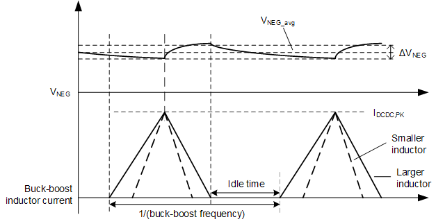
The buck-boost converter uses a peak current hysteretic control. As shown in Figure 8-2, the inductor current increases at the beginning of a switching cycle until the inductor reaches the peak current limit. Then the inductor current goes down to zero. The idle time between each current pulse is determined automatically by the buck-boost controller, and can be reduced to zero. Therefore, the maximum output current happens when the idle time is zero, and is decided by the peak current but to a first order is independent of the inductor value. However, the peak output current the buck-boost can deliver to the -14V rail is proportional to the VDD input voltage. Therefore, the maximum switching frequency of the GaN that the buck-boost can support varies with VDD voltage and is only specified for operation up to 2 MHz for VDD voltages above 9V.
 Figure 8-2 Buck-Boost Converter Inductor
Current
Figure 8-2 Buck-Boost Converter Inductor
CurrentThe LMG3522R030 supports the GaN operation up to 2 MHz. As power consumption is very different in a wide switching frequency range enabled by the GaN device, two peak current limits are used to control the buck-boost converter. The two ranges are separated by IN positive-going threshold frequency. As shown in Figure 8-3, when switching frequency is in the lower range, the peak current is initially set to the lower value IBBSW,M(low) (typically 0.4 A) . When switching frequency is in the higher range, the peak current is raised to the higher value IBBSW,M(high) (typically 1 A) and requires a larger inductor. There is a filter on this frequency detection logic, therefore the LMG3522R030 requires five consecutive cycles at the higher frequency before it is set to the higher buck-boost peak current limit. The current limit does not go down again until power off after the higher limit is set. Even if the switching frequency returns to the lower range, the current limit does not decrease to the lower limit.
As the peak current of the buck-boost is subject to two different peak current limits which are 0.4 A and 1 A for low and high frequency operation (see Internal Buck-Boost DC-DC Converter), so the inductor must have a saturation current well above the rated peak current limit. After the higher limit is established by switching at a higher frequency, the current limit does not go back to the lower level even when GaN device is then switched at a lower frequency. Therefore, selecting an inductor according to the higher 1-A limit is recommended.