ZHCSQH3 November 2022 LMG3522R030
PRODUCTION DATA
- 1 特性
- 2 应用
- 3 说明
- 4 Revision History
- 5 Pin Configuration and Functions
- 6 Specifications
- 7 Parameter Measurement Information
-
8 Detailed Description
- 8.1 Overview
- 8.2 Functional Block Diagram
- 8.3
Feature Description
- 8.3.1 GaN FET Operation Definitions
- 8.3.2 Direct-Drive GaN Architecture
- 8.3.3 Drain-Source Voltage Capability
- 8.3.4 Internal Buck-Boost DC-DC Converter
- 8.3.5 VDD Bias Supply
- 8.3.6 Auxiliary LDO
- 8.3.7 Fault Detection
- 8.3.8 Drive Strength Adjustment
- 8.3.9 Temperature-Sensing Output
- 8.3.10 Ideal-Diode Mode Operation
- 8.4 Start Up Sequence
- 8.5 Safe Operation Area (SOA)
- 8.6 Device Functional Modes
- 9 Application and Implementation
- 10Device and Documentation Support
- 11Mechanical, Packaging, and Orderable Information
9.4.2.2 Managing the Bootstrap Voltage
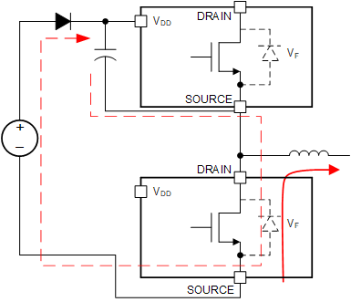
In a synchronous buck or other converter where the low-side switch occasionally operates in third-quadrant, the bootstrap supply charges through a path that includes the third-quadrant voltage drop of the low-side LMG3522R030 during the dead time as shown in Figure 9-7. This third-quadrant drop can be large, which can over-charge the bootstrap supply in certain conditions. The VDD supply of LMG3522R030 must be kept below 18 V.
 Figure 9-7 Charging Path for Bootstrap Diode
As shown in Figure 9-8, the recommended bootstrap supply includes a bootstrap diode, a series resistor, and a 16-V TVS or zener diode in parallel with the VDD bypass capacitor to prevent damaging the high-side LMG3522R030. The series resistor limits the charging current at start-up and when the low-side device is operating in third-quadrant mode. This resistor must be selected to allow sufficient current to power the LMG3522R030 at the desired operating frequency. At 100-kHz operation, TI recommends a value of approximately 2 Ω . At higher frequencies, this resistor value must be reduced or the resistor omitted entirely to ensure sufficient supply current.
 Figure 9-8 Suggested Bootstrap Regulation Circuit