ZHCST00 september   2023 LMG3522R050

PRODUCTION DATA  

  1.   1
  2. 特性
  3. 应用
  4. 说明
  5. Revision History
  6. Pin Configuration and Functions
  7. Specifications
    1. 6.1 Absolute Maximum Ratings
    2. 6.2 ESD Ratings
    3. 6.3 Recommended Operating Conditions
    4. 6.4 Thermal Information
    5. 6.5 Electrical Characteristics
    6. 6.6 Switching Characteristics
    7. 6.7 Typical Characteristics
  8. Parameter Measurement Information
    1. 7.1 Switching Parameters
      1. 7.1.1 Turn-On Times
      2. 7.1.2 Turn-Off Times
      3. 7.1.3 Drain-Source Turn-On Slew Rate
  9. Detailed Description
    1. 8.1 Overview
    2. 8.2 Functional Block Diagram
    3. 8.3 Feature Description
      1. 8.3.1  GaN FET Operation Definitions
      2. 8.3.2  Direct-Drive GaN Architecture
      3. 8.3.3  Drain-Source Voltage Capability
      4. 8.3.4  Internal Buck-Boost DC-DC Converter
      5. 8.3.5  VDD Bias Supply
      6. 8.3.6  Auxiliary LDO
      7. 8.3.7  Fault Detection
        1. 8.3.7.1 Overcurrent Protection and Short-Circuit Protection
        2. 8.3.7.2 Overtemperature Shutdown
        3. 8.3.7.3 UVLO Protection
        4. 8.3.7.4 Fault Reporting
      8. 8.3.8  Drive-Strength Adjustment
      9. 8.3.9  Temperature-Sensing Output
      10. 8.3.10 Ideal-Diode Mode Operation
        1. 8.3.10.1 Overtemperature-Shutdown Ideal-Diode Mode
    4. 8.4 Start-Up Sequence
    5. 8.5 Safe Operation Area (SOA)
      1. 8.5.1 Repetitive SOA
    6. 8.6 Device Functional Modes
  10. Application and Implementation
    1. 9.1 Application Information
    2. 9.2 Typical Application
      1. 9.2.1 Design Requirements
      2. 9.2.2 Detailed Design Procedure
        1. 9.2.2.1 Slew Rate Selection
          1. 9.2.2.1.1 Start-Up and Slew Rate With Bootstrap High-Side Supply
        2. 9.2.2.2 Signal Level-Shifting
        3. 9.2.2.3 Buck-Boost Converter Design
      3. 9.2.3 Application Curves
    3. 9.3 Do's and Don'ts
    4. 9.4 Power Supply Recommendations
      1. 9.4.1 Using an Isolated Power Supply
      2. 9.4.2 Using a Bootstrap Diode
        1. 9.4.2.1 Diode Selection
        2. 9.4.2.2 Managing the Bootstrap Voltage
    5. 9.5 Layout
      1. 9.5.1 Layout Guidelines
        1. 9.5.1.1 Solder-Joint Reliability
        2. 9.5.1.2 Power-Loop Inductance
        3. 9.5.1.3 Signal-Ground Connection
        4. 9.5.1.4 Bypass Capacitors
        5. 9.5.1.5 Switch-Node Capacitance
        6. 9.5.1.6 Signal Integrity
        7. 9.5.1.7 High-Voltage Spacing
        8. 9.5.1.8 Thermal Recommendations
      2. 9.5.2 Layout Examples
  11. 10Device and Documentation Support
    1. 10.1 Documentation Support
      1. 10.1.1 Related Documentation
    2. 10.2 接收文档更新通知
    3. 10.3 支持资源
    4. 10.4 Trademarks
    5. 10.5 静电放电警告
    6. 10.6 Export Control Notice
    7. 10.7 术语表

封装选项

机械数据 (封装 | 引脚)
散热焊盘机械数据 (封装 | 引脚)
订购信息

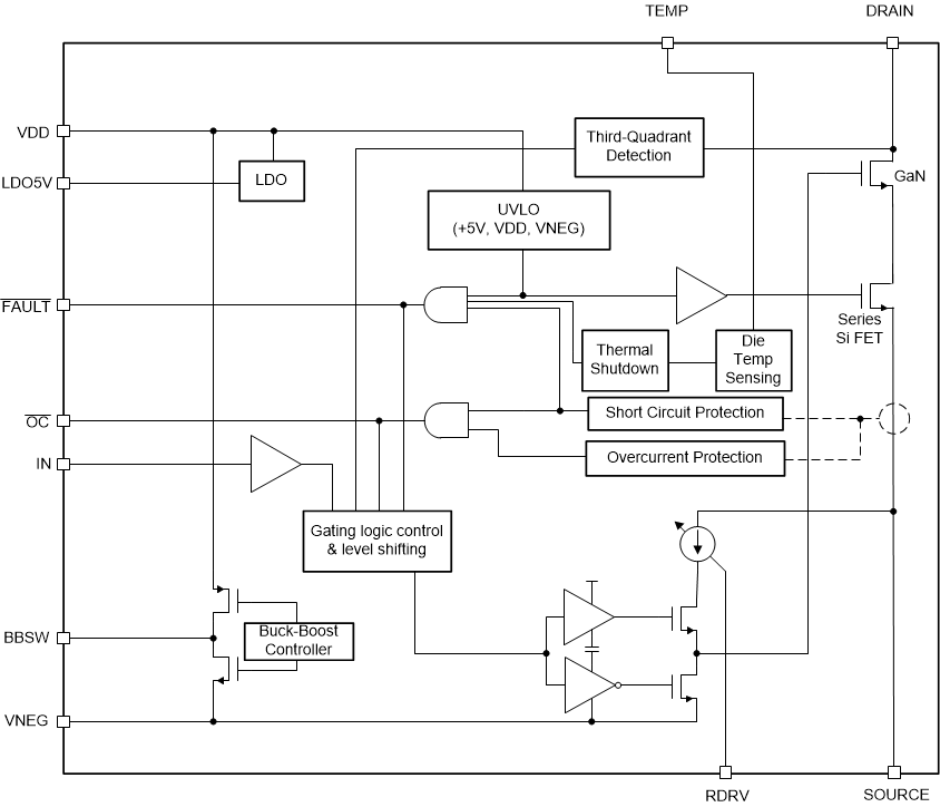
Functional Block Diagram

GUID-FCA67097-3F17-4C5C-84C8-8C769137DCCC-low.gif