ZHCSFT3D March 2015 – March 2017 LMG5200
PRODUCTION DATA.
9 Application and Implementation
NOTE
Information in the following applications sections is not part of the TI component specification, and TI does not warrant its accuracy or completeness. TI’s customers are responsible for determining suitability of components for their purposes. Customers should validate and test their design implementation to confirm system functionality.
9.1 Application Information
The LMG5200 GaN power stage is a versatile building block for various types of high-frequency, switch-mode power applications. The high-performance gate driver IC integrated in the package helps minimize the parasitics and results in extremely fast switching of the GaN FETs. The device design is highly optimized for synchronous buck converters and other half-bridge configurations.
9.2 Typical Application
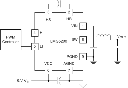
Figure 11 shows a synchronous buck converter application with VCC connected to a 5-V supply. It is critical to optimize the power loop (loop impedance from VIN capacitor to PGND). Having a high power loop inductance causes significant ringing in the SW node and also causes the associated power loss. Refer to the Layout Guidelines section for information on how to minimize this power loop.
 Figure 11. Typical Connection Diagram For a Synchronous Buck Converter
9.2.1 Design Requirements
When designing a synchronous buck converter application that incorporates the LMG5200 power stage, some design considerations must be evaluated first to make the most appropriate selection. Among these considerations are the input voltages, passive components, operating frequency, and controller selection.Table 4 shows some sample values for a typical application. See Power Supply Recommendations, Layout, and Power Dissipation for other key design considerations for the LMG5200.
Table 4. Design Parameters
| PARAMETER | SAMPLE VALUE | |||
|---|---|---|---|---|
| Half-bridge input supply voltage, VIN | 48 V | |||
| Output voltage, VOUT | 12 V | |||
| Output current | 8 A | |||
| VHB-HS bootstrap capacitor | 0.1 uF, X5R | |||
| Switching frequency | 1 MHz | |||
| Dead time | 8 ns | |||
| Inductor | 4.7 µH | |||
| Controller | TPS40400 | |||
9.2.2 Detailed Design Procedure
This procedure outlines the design considerations of LMG5200 in a synchronous buck converter. For additional design help, see 相关文档.
9.2.2.1 VCC Bypass Capacitor
The VCC bypass capacitor provides the gate charge for the low-side and high-side transistors and to absorb the reverse recovery charge of the bootstrap diode. The required bypass capacitance can be calculated with Equation 1.
QgH and QgL are the gate charge of the high-side and low-side transistors, respectively. Qrr is the reverse recovery charge of the bootstrap diode. ΔV is the maximum allowable voltage drop across the bypass capacitor. A 0.1-µF or larger value, good-quality, ceramic capacitor is recommended. Place the bypass capacitor as close as possible to the VCC and AGND pins of the device to minimize the parasitic inductance.
9.2.2.2 Bootstrap Capacitor
The bootstrap capacitor provides the gate charge for the high-side gate drive, dc bias power for HB UVLO circuit, and the reverse recovery charge of the bootstrap diode. The required bypass capacitance can be calculated using Equation 2.
where
- IHB is the quiescent current of the high-side gate driver (150 µA, maximum)
- tON(maximum) is the maximum on-time period of the high-side gate driver
- Qrr is the reverse recovery charge of the bootstrap diode
- QgH is the gate charge of the high-side GaN FET
- ΔV is the permissible ripple in the bootstrap capacitor (< 100 mV, typical)
A 0.1-µF, 16-V, 0402 ceramic capacitor is suitable for most applications. Place the bootstrap capacitor as close as possible to the HB and HS pins.
9.2.2.3 Power Dissipation
Ensure that the power loss in the driver and the GaN FETs is maintained below the maximum power dissipation limit of the package at the operating temperature. The smaller the power loss in the driver and the GaN FETs, the higher the maximum operating frequency that can be achieved in the application. The total power dissipation of the LMG5200 device is the sum of the gate driver losses, the bootstrap diode power loss and the switching and conduction losses in the FETs.
The gate driver losses are incurred by charge and discharge of the capacitive load. It can be approximated using Equation 3.

where
- Qg is the gate charge
- VDD is the bias supply
- fSW is the switching frequency
There are some additional losses in the gate drivers due to the internal CMOS stages used to buffer the outputs. Figure 1 shows the measured gate driver power dissipation versus frequency and load capacitance. Use this graph to approximate the power losses due to the gate drivers.
The bootstrap diode power loss is the sum of the forward bias power loss that occurs while charging the bootstrap capacitor and the reverse bias power loss that occurs during reverse recovery. Because each of these events happens once per cycle, the diode power loss is proportional to the operating frequency. Higher input voltages (VIN) to the half bridge also result in higher reverse recovery losses.
The power losses due to the GaN FETs can be divided into conduction losses and switching losses. Conduction losses are resistive losses and can be calculated using Equation 4.

where
- RDS(on)HS is the high-side GaN FET on-resistance
- RDS(on)LS is the low-side GaN FET on-resistance
- IRMS(HS) is the high-side GaN FET RMS current
- IRMS(LS) and low-side GaN FET RMS current
The switching losses can be computed to a first order using Equation 5.

where
- tTR is the switch transition time from ON to OFF and from OFF to ON
Note that the low-side FET does not suffer from this loss. The third quadrant loss in the low-side device is ignored in this first order loss calculation.
As described previously, switching frequency has a direct effect on device power dissipation. Although the gate driver of the LMG5200 device is capable of driving the GaN FETs at frequencies up to 10 MHz, careful consideration must be applied to ensure that the running conditions for the device meet the recommended operating temperature specification. Specifically, hard-switched topologies tend to generate more losses and self-heating than soft-switched applications.
The sum of the driver loss, the bootstrap diode loss, and the switching and conduction losses in the GaN FETs is the total power loss of the device. Careful board layout with an adequate amount of thermal vias close to the power pads (VIN and PGND) allows optimum power dissipation from the package. A top-side mounted heat sink with airflow can also improve the package power dissipation.
9.2.3 Application Curves
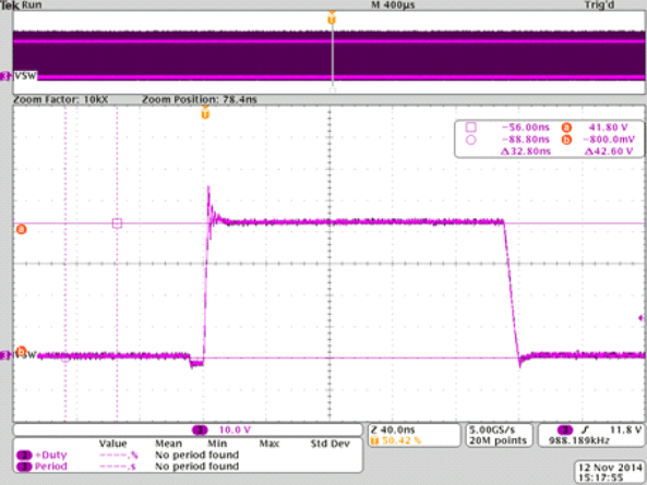
 Figure 12. SW Node Behavior Showing the Dead Time
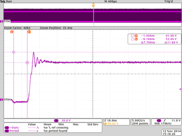
 Figure 13. Zoom-In Showing the Dead Time of 7.7 ns and the Overshoot of the SW Node