ZHCSFT3D March 2015 – March 2017 LMG5200
PRODUCTION DATA.
6 Specifications
6.1 Absolute Maximum Ratings
over operating free-air temperature range (unless otherwise noted)(1)| PARAMETER | MIN | MAX | UNIT |
|---|---|---|---|
| VIN to PGND | 0 | 80 | V |
| VIN to PGND (pulsed, 100-ms maximum duration)(2) | 100 | V | |
| HB to AGND | –0.3 | 86 | V |
| HS to AGND | –5 | 80 | V |
| HI to AGND | –0.3 | 12 | V |
| LI to AGND | –0.3 | 12 | V |
| VCC to AGND | –0.3 | 6 | V |
| HB to HS | –0.3 | 6 | V |
| HB to VCC | 0 | 80 | V |
| SW to PGND | –5 | 80 | V |
| IOUT from SW pin | 10 | A | |
| Junction temperature, TJ | –40 | 125 | °C |
| Storage temperature, Tstg | –40 | 150 | °C |
(1) Stresses beyond those listed under Absolute Maximum Ratings may cause permanent damage to the device. These are stress ratings only, which do not imply functional operation of the device at these or any other conditions beyond those indicated under Recommended Operating Conditions. Exposure to absolute-maximum-rated conditions for extended periods may affect device reliability.
(2) Device can withstand 1000 pulses up to 100 V of 100-ms duration and less than 1% duty cycle over its lifetime.
6.2 ESD Ratings
| VALUE | UNIT | |||
|---|---|---|---|---|
| V(ESD) | Electrostatic discharge | Human-body model (HBM), per ANSI/ESDA/JEDEC JS-001(1) | ±1000 | V |
| Charged-device model (CDM), per JEDEC specification JESD22-C101(2) |
±500 | V | ||
(1) JEDEC document JEP155 states that 500-V HBM allows safe manufacturing with a standard ESD control process.
(2) JEDEC document JEP157 states that 250-V CDM allows safe manufacturing with a standard ESD control process.
6.3 Recommended Operating Conditions
over operating free-air temperature range (unless otherwise noted)| MIN | NOM | MAX | UNIT | ||
|---|---|---|---|---|---|
| VCC | 4.75 | 5 | 5.25 | V | |
| LI or HI Input | 0 | 12 | V | ||
| VIN | 0 | 80 | V | ||
| HS, SW | –5 | 80 | V | ||
| HB | VHS + 4 | VHS + 5.25 | V | ||
| HS, SW slew rate(1) | 50 | V/ns | |||
| Junction temperature, TJ | –40 | 125 | °C | ||
(1) This parameter is ensured by design. Not tested in production.
6.4 Thermal Information
| THERMAL METRIC (1) (2) | LMG5200 | UNIT | |
|---|---|---|---|
| MOF (QFM) | |||
| 9 PINS | |||
| R θJA | Junction-to-ambient thermal resistance | 35 | °C/W |
| R θJC(top) | Junction-to-case (top) thermal resistance | 18 | °C/W |
| R θJB | Junction-to-board thermal resistance | 16 | °C/W |
| ψ JT | Junction-to-top characterization parameter | 1.8 | °C/W |
| ψ JB | Junction-to-board characterization parameter | 16 | °C/W |
(1) For more information about traditional and new thermal metrics, see the Semiconductor and IC Package Thermal Metrics application report.
(2) For thermal estimates of this device based on PCB copper area, see the TI PCB Thermal Calculator .
6.5 Electrical Characteristics
over operating free-air temperature range (unless otherwise noted)(1)| PARAMETER | TEST CONDITIONS | MIN | TYP | MAX | UNIT | |
|---|---|---|---|---|---|---|
| SUPPLY CURRENTS | ||||||
| ICC | VCC quiescent current | LI = HI = 0 V, VCC = 5 V, HB-HS = 4.6 V | 0.08 | 0.125 | mA | |
| ICCO | Total VCC operating current | f = 500 kHz | 3 | 5 | mA | |
| IHB | HB quiescent current | LI = HI = 0 V, VCC = 5 V, HB-HS = 4.6 V | 0.09 | 0.15 | mA | |
| IHBO | HB operating current | f = 500 kHz, 50% Duty cycle, VDD = 5 V | 1.5 | 2.5 | mA | |
| INPUT PINS | ||||||
| VIH | High-level input voltage threshold | Rising edge | 1.87 | 2.06 | 2.22 | V |
| VIL | Low-level input voltage threshold | Falling edge | 1.48 | 1.66 | 1.76 | V |
| VHYS | Hysteresis between rising and falling threshold | 400 | mV | |||
| RI | Input pulldown resistance | 100 | 200 | 300 | kΩ | |
| UNDERVOLTAGE PROTECTION | ||||||
| VCCR | VCC Rising edge threshold | Rising | 3.2 | 3.8 | 4.5 | V |
| VCC(hyst) | VCC UVLO threshold hysteresis | 200 | mV | |||
| VHBR | HB Rising edge threshold | Rising | 2.5 | 3.2 | 3.9 | V |
| VHB(hyst) | HB UVLO threshold hysteresis | 200 | mV | |||
| BOOTSTRAP DIODE | ||||||
| VDL | Low-current forward voltage | IVDD-HB = 100 µA | 0.45 | 0.65 | V | |
| VDH | High current forward voltage | IVDD-HB = 100 mA | 0.9 | 1.0 | V | |
| RD | Dynamic resistance | IVDD-HB = 100 mA | 1.85 | 2.8 | Ω | |
| HB-HS clamp | Regulation Voltage | 4.65 | 5 | 5.2 | V | |
| tBS | Bootstrap diode reverse recovery time | IF = 100 mA, IR = 100 mA | 40 | ns | ||
| QRR | Bootstrap diode reverse recovery charge | VVIN = 50 V | 2 | nC | ||
| POWER STAGE | ||||||
| RDS(ON)HS | High-side GaN FET on-resistance | LI = 0 V, HI = VCC=5 V, HB-HS = 5 V, VIN-SW = 10 A, TJ = 25℃ | 15 | 20 | mΩ | |
| RDS(ON)LS | Low-side GaN FET on-resistance | LI = VCC = 5V, HI = 0 V, HB-HS = 5 V, SW-PGND = 10 A, TJ = 25℃ | 15 | 20 | mΩ | |
| VSD | GaN 3rd quadrant conduction drop | ISD = 500 mA, VIN floating, VVCC = 5 V, HI = LI = 0 V | 2 | V | ||
| IL-VIN-SW | Leakage from VIN to SW when the high-side GaN FET and low-side GaN FET are off | VIN = 80 V, HI = LI = 0 V, VVCC = 5 V, TJ= 25℃ | 25 | 150 | µA | |
| IL-SW-GND | Leakage from SW to GND when the high-side GaN FET and low-side GaN FET are off | SW = 80 V, HI = LI = 0 V, VVCC = 5V, TJ = 25℃ | 25 | 150 | µA | |
| COSS | Output capacitance of high-side GaN FET and low-side GaN FET | VDS=40 V, VGS= 0V (HI = LI = 0 V) | 266 | pF | ||
| QG | Total gate charge | VDS=40 V, ID= 10A, VGS= 5 V | 3.8 | nC | ||
| QOSS | Output charge | VDS=40 V, ID= 10 A | 21 | nC | ||
| QRR | Source-to-drain reverse recovery charge | Not including internal driver bootstrap diode | 0 | nC | ||
| tHIPLH | Propagation delay: HI rising(2) | LI = 0 V, VCC = 5 V, HB-HS = 5 V, VIN = 30 V | 29.5 | 50 | ns | |
| tHIPHL | Propagation delay: HI falling(2) | LI = 0 V, VCC = 5 V, HB-HS = 5 V, VIN = 30 V | 29.5 | 50 | ns | |
| tLPLH | Propagation delay: LI rising(2) | HI = 0 V, VCC = 5 V, HB-HS = 5 V, VIN = 30 V | 29.5 | 50 | ns | |
| tLPHL | Propagation delay: LI falling(2) | HI = 0 V, VCC = 5 V, HB-HS = 5 V, VIN = 30 V | 29.5 | 50 | ns | |
| tMON | Delay matching: LI high and HI low(2) | 2 | 8 | ns | ||
| tMOFF | Delay matching: LI low and HI high(2) | 2 | 8 | ns | ||
| tPW | Minimum input pulse width that changes the output | 10 | ns | |||
(1) Parameters that show only a typical value are ensured by design and may not be tested in production.
6.6 Typical Characteristics
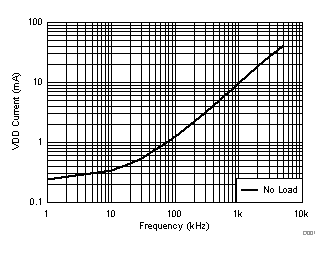
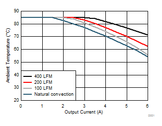
All the curves are based on measurements made on a PCB design with dimensions of 3.2 inches (W) × 2.7 inches (L) × 0.062 inch (T) and 4 layers of 2 oz copper.
| VDD = 5 V |

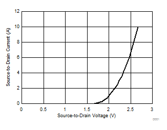
GaN third quadrant conduction.
Figure 3. Source-to-Drain Current vs Source-to-Drain Voltage

| VIN = 48 V | VOUT = 5 V | fSW = 1 MHz |

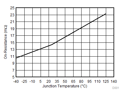
.
Figure 4. GaN FET On-Resistance vs Junction Temperature