SNLS285H April 2008 – May 2016 LMH0303
PRODUCTION DATA.
- 1 Features
- 2 Applications
- 3 Description
- 4 Revision History
- 5 Pin Configuration and Functions
- 6 Specifications
- 7 Detailed Description
- 8 Application and Implementation
- 9 Power Supply Recommendations
- 10Layout
- 11Device and Documentation Support
- 12Mechanical, Packaging, and Orderable Information
10 Layout
10.1 Layout Guidelines
TI recommends the following layout guidelines for the LMH0303:
- The RREF 1% tolerance resistor should be placed as close as possible to the RREF pin. In addition, the copper in the plane layers below the RREF network should be removed to minimize parasitic capacitance.
- Choose a suitable board stackup that supports 75-Ω single-ended trace and 100-Ω differential trace routing on the top layer of the board. This is typically done with a Layer 2 ground plane reference for the 100-Ω differential traces and a second ground plane at Layer 3 reference for the 75-Ω single-ended traces.
- Use single-ended uncoupled trace designed with 75-Ω impedance for signal routing to SDO and SDO. The trace width is typically 8-10 mil reference to a ground plane at Layer 3.
- Use coupled differential traces with 100-Ω impedance for signal routing to SDI and SDI. They are usually 5-mil to 8-mil trace width reference to a ground plane at Layer 2.
- Place anti-pad (ground relief) on the power and ground planes directly under the 4.7-μF AC-coupling capacitor, return loss network, and IC landing pads to minimize parasitic capacitance. The size of the anti-pad depends on the board stackup and can be determined by a 3-dimension electromagnetic simulation tool.
- Use a well-designed BNC footprint to ensure the BNC’s signal landing pad achieves 75-Ω characteristic impedance. BNC suppliers usually provide recommendations on BNC footprint for best results.
- Keep trace length short between the BNC and SDO. The trace routing for SDO and SDO should be symmetrical, approximately equal lengths, and equal loading.
- The exposed pad EP of the package should be connected to the ground plane through an array of vias. These vias are solder-masked to avoid solder flow into the plated-through holes during the board manufacturing process.
- Connect each supply pin (VCC and VEE) to the power or ground planes with a short via. The via is usually placed tangent to the landing pads of the supply pins with the shortest trace possible.
- Power-supply bypass capacitors should be placed close to the supply pins.
10.2 Layout Example
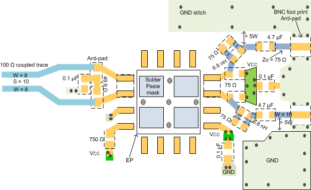
Figure 8 shows an example of proper layout requirements for the LMH0303.
 Figure 8. LMH0303 High-Speed Traces Layout Example