SNLS308G April 2009 – June 2015 LMH0384
PRODUCTION DATA.
- 1 Features
- 2 Applications
- 3 Description
- 4 Revision History
- 5 Pin Configuration and Functions
- 6 Specifications
- 7 Detailed Description
- 8 Application and Implementation
- 9 Power Supply Recommendations
- 10Layout
- 11Device and Documentation Support
- 12Mechanical, Packaging, and Orderable Information
10 Layout
10.1 Layout Guidelines
For information on layout and soldering of the WQFN package, please refer to the following application note: AN-1187 Leadless Leadframe Package (LLP) (SNOA401).
The ST 424, 292, and 259 standards have stringent requirements for the input return loss of receivers, which essentially specify how closely the input must resemble a 75-Ω network. Any non-idealities in the network between the BNC and the equalizer will degrade the input return loss. Take care to minimize impedance discontinuities between the BNC and the equalizer to ensure that the characteristic impedance of this trace is 75 Ω.
Please consider the following PCB recommendations:
- Use surface-mount components, and use the smallest components available. In addition, use the smallest size component pads.
- Select trace widths that minimize the impedance mismatch between the BNC and the equalizer.
- Select a board stack up that supports both 75-Ω single-ended traces and 100-Ω loosely-coupled differential traces.
- Place return loss components closest to the equalizer input pins.
- Maintain symmetry on the complementary signals.
- Route 100-Ω traces uniformly (keep trace widths and trace spacing uniform along the trace).
- Avoid sharp bends in the signal path; use 45° or radial bends.
- Place bypass capacitors close to each power pin, and use the shortest path to connect equalizer power and ground pins to the respective power or ground planes.
10.2 Layout Example
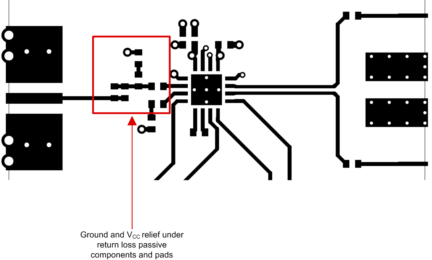
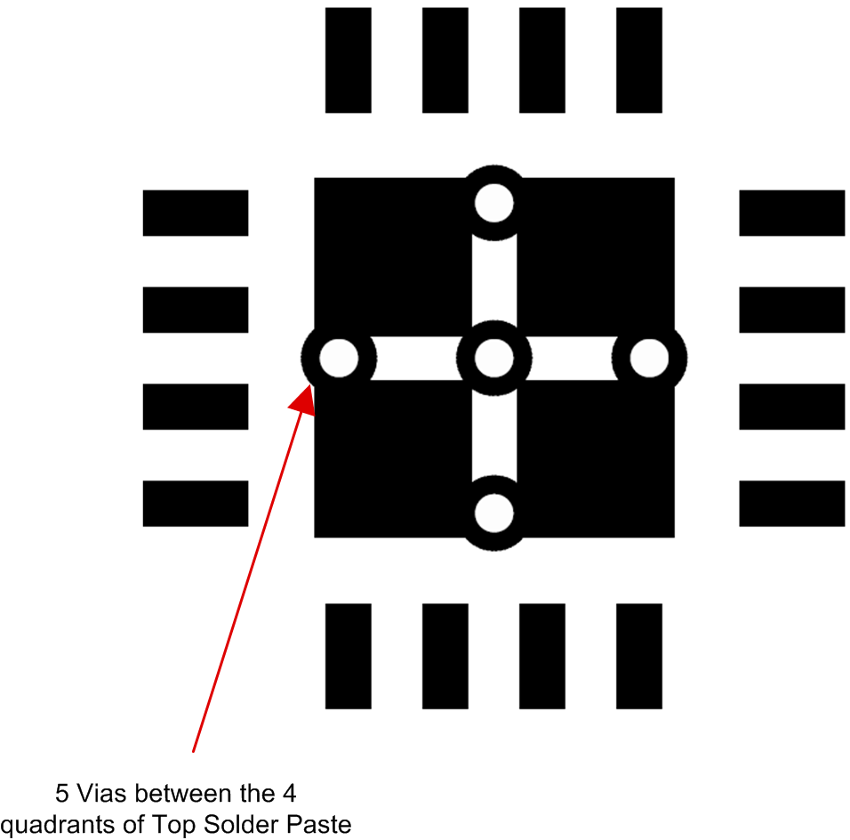
Figure 15 and Figure 16 demonstrate the LMH0384EVM PCB layout. Ground and supply relief under the return loss passive components and pads reduces parasitic - improving return loss performance. Note 5 vias without solder paste are located between 4 squares solder paste mainly for thermal as well as to improve soldering during board assembly.
 Figure 15. LMH0384EVM Top Etch Layout Example
 Figure 16. LMH384EVM Top Solder Paste Mask