SNLS323N August 2010 – January 2017 LMH0395
PRODUCTION DATA.
- 1 Features
- 2 Applications
- 3 Description
- 4 Revision History
- 5 Pin Configuration and Functions
- 6 Specifications
-
7 Detailed Description
- 7.1 Overview
- 7.2 Functional Block Diagram
- 7.3 Feature Description
- 7.4 Device Functional Modes
- 7.5
Programming
- 7.5.1
SPI Register Access
- 7.5.1.1 SPI Transaction Overview
- 7.5.1.2 SPI Write
- 7.5.1.3 SPI Read
- 7.5.1.4 SPI Daisy-Chain Operation
- 7.5.1.5 SPI Daisy-Chain Write
- 7.5.1.6 SPI Daisy-Chain Read
- 7.5.1.7 SPI Daisy-Chain Read and Write Example
- 7.5.1.8 SPI Daisy-Chain Length Detection
- 7.5.1.9 Output Driver Adjustments and De-Emphasis Setting
- 7.5.1.10 Launch Amplitude Optimization
- 7.5.1.11 Cable Length Indicator (CLI)
- 7.5.1
SPI Register Access
- 7.6 Register Maps
- 8 Application and Implementation
- 9 Power Supply Recommendations
- 10Layout
- 11Device and Documentation Support
- 12Mechanical, Packaging, and Orderable Information
7 Detailed Description
7.1 Overview
The LMH0395 is a 3-Gbps HD/SD SDI low power extended reach adaptive cable equalizer. It is designed to equalize data transmitted over cable or any media with similar dispersive loss characteristics.. The equalizer operates over a wide range of data rates from 125 Mbps to 2.97 Gbps and supports ST 424, ST 292, ST 344, ST 259, and DVB-ASI standards. The LMH0395 provides extended cable reach with improved immunity to crosstalk and ultra-low power consumption. The LMH0395 equalizer features active sensing features and design enhancements including longer cable equalization, lower output jitter, configurable pin mode and SPI modes, a power-saving sleep mode, and programmable output common-mode voltage and swing. The LMH0395 implements DC restoration to correctly handle pathological data conditions.
The LMH0395 includes power management to further reduce power consumption when no input signal is present. The output driver offers programmable de-emphasis for up to 40” of FR4 trace losses.
7.2 Functional Block Diagram
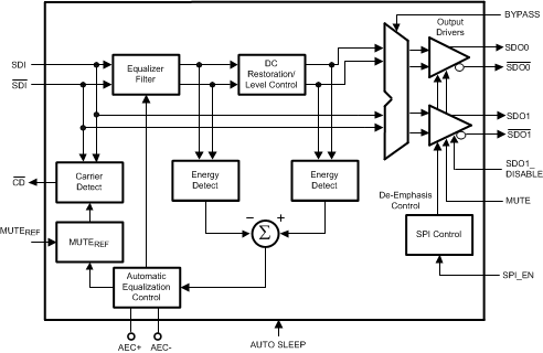
The LMH0395 supports two modes of operation. In pin mode, the LMH0395 operates with control pins to set its operating state. In SPI mode, an optional SPI serial interface can be used to access and configure multiple LMH0395 devices in a daisy-chain configuration.
This allows users to program the output common-mode voltage and swing, output de-emphasis level, input launch amplitude, and power management settings. Users may also access a cable length indicator and all pin mode features.
7.3 Feature Description
The Equalizer Filter block is a multi-stage adaptive filter. If Bypass is high, the equalizer filter is disabled.
The DC Restoration / Level Control block receives the differential signals from the equalizer filter block. This block incorporates a self-biasing DC restoration circuit to fully DC restore the signals. If Bypass is high, this function is disabled.
The signals before and after the DC Restoration / Level Control block are used to generate the Automatic Equalization Control (AEC) signal. This control signal sets the gain and bandwidth of the equalizer filter.
The Carrier Detect block generates the carrier detect signal based on the SDI input and an adjustment from the Mute Reference block.
The SPI Control block uses the MOSI, MISO, SCK, and SS signals in SPI mode to control the SPI registers. SPI_EN selects between SPI mode and pin mode. Driving SPI_EN low enables pin mode.
The Output Drivers produce SDO0, SDO0, SDO1, and SDO1.
7.3.1 Mute Reference (MuteREF)
The mute reference sets the threshold for CD and (with CD tied to MUTE) determines the amount of cable to equalize before automatically muting the outputs. This is set by applying a voltage inversely proportional to the length of cable to equalize. The applied voltage must be greater than the MUTEREF floating voltage (typically 1.3 V) in order to change the CD threshold. As the applied MUTEREF voltage is increased, the amount of cable that can be equalized before carrier detect is de-asserted and the outputs are muted is decreased. MUTEREF may be left unconnected or connected to ground for normal CD operation. Optionally, the LMH0395 allows the mute reference to be set digitally through SPI register 03h.
Figure 6 shows the minimum MUTEREF input voltage required to force carrier detect to inactive vs. Belden 1694A cable length. The results shown are valid for Belden 1694A cable lengths of 0-200 m at 2.97 Gbps, 0-220 m at 1.485 Gbps, and 0-400 m at 270 Mbps.
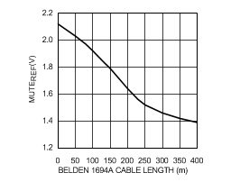 Figure 6. MuteREF vs. Belden 1694a Cable Length
7.3.2 Carrier Detect (CD) and Mute
Carrier detect CD indicates if a valid signal is present at the LMH0395 input. This signal is a logical OR operation of internal energy detector and MUTEREF setting (if used). Internal energy detector detects energy across different data rates. If MUTEREF is used, the carrier detect threshold will be altered accordingly. CD provides a high voltage when no signal is present at the LMH0395 input. CD is low when a valid input signal is detected.
MUTE can be used to manually mute or enable the output drivers. Applying a high input to MUTE will mute the LMH0395 outputs by forcing the output to a logic 1. Applying a low input will force the outputs to be active.
In pin mode, CD and MUTE may be tied together to automatically mute the output when no input signal is present.
7.3.3 Input Interfacing
The LMH0395 accepts single-ended input. The input must be AC coupled. The Functional Block Diagram diagram shows the typical configuration for a single-ended input. The unused input must be properly terminated as shown in Figure 7 or Figure 8.
The LMH0395 can be optimized for different launch amplitudes through the SPI (see Launch Amplitude Optimization in the SPI Register Access section).
The LMH0395 correctly handles equalizer pathological signals for standard definition and high definition serial digital video, as described in ST RP 178 and RP 198, respectively.
7.3.4 Output Interfacing
The LMH0395 dual output differential pairs, SDO0, SDO0, SDO1, and SDO1 are internally terminated 100-Ω LVDS outputs. These outputs can be DC coupled to most common differential receivers.
The default output common-mode voltage (VOS) is 1.2 V. The output common-mode voltage may be adjusted through the SPI in 200 mV increments, from 0.8 V to 1.2 V (see Output Driver Adjustments and De-Emphasis Setting in the SPI Register Access section). When the output common mode is supply referenced, the common-mode voltage is about 1.35 V (for 700 mVP-P differential swing). This adjustable output common-mode voltage offers flexibility for interfacing to many types of receivers.
The default differential output swing (VSSP-P) is 700 mVP-P. The differential output swing may be adjusted through the SPI. Valid options are 400, 600, 700, or 800 mVP-P (see Output Driver Adjustments and De-Emphasis Setting in the SPI Register Access section).
The LMH0395 output should be DC coupled to the input of the receiving device where possible. 100-Ω differential transmission lines should be used to connect between the LMH0395 outputs and the input of the receiving device.
The LMH0395 output should not be DC coupled to CML inputs. If there are strong pull-up resistors (that is, 50 Ω) at the receiving device, AC coupling should be used. The value of these AC-coupling capacitors should be large enough (typically 4.7 µF) to accommodate for the SD pathological video pattern.
Figure 7 shows an example of a DC-coupled interface between the LMH0395 and LMH0346 SDI reclocker. The differential transmission line should be terminated with a 100-Ω resistor at the receiving device as shown. The resistor should be placed as close as possible to the LMH0346 input. If desired, this network may be terminated with two 50-Ω resistors and a center-tap capacitor to ground in place of the single 100-Ω resistor.
Figure 8 shows an example of a DC-coupled interface between the LMH0395 and LMH0356 SDI reclocker. The LMH0356 inputs have internal 50-Ω terminations (100 Ω differential) to terminate the transmission line, so no additional components are required.
The LMH0395 output drivers are equipped with programmable output de-emphasis to minimize inter-symbol interference caused by the loss dispersion from driving signals across PCB traces (see Output Driver Adjustments and De-Emphasis Setting in the SPI Register Access section). De-emphasis works with all combinations of output common-mode voltage and output voltage swing settings to support DC coupling to the receiving device.
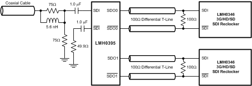 Figure 7. DC Output Interface To LMH0346 Reclocker
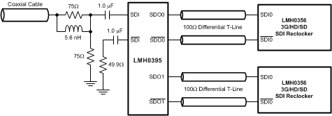 Figure 8. DC Output Interface To LMH0356 Reclocker
7.4 Device Functional Modes
The LMH0395 supports two modes of operation. In pin mode, the LMH0395 operates with control pins to set its operating state. In SPI mode, an optional SPI serial interface can be used to access and configure multiple LMH0395 devices in a daisy-chain configuration.
This allows users to program the output common-mode voltage and swing, output de-emphasis level, input launch amplitude, and power management settings. Users may also access a cable length indicator and all pin mode features.
7.4.1 Auto Sleep
The auto sleep mode allows the LMH0395 to power down when no input signal is detected. If the AUTO SLEEP pin is set high, the LMH0395 goes into a deep power-save mode when no signal is detected. The device powers on again once an input signal is detected. If the AUTO SLEEP pin is set low, the LMH0395 will always be on and will not enter power-save mode. The auto sleep functionality can be turned off by setting AUTO SLEEP low or tying this pin to ground. An additional auto sleep setting available in SPI mode can be used to force the equalizer to power down regardless of whether there is an input signal or not. Auto sleep has precedence over mute and bypass modes.
In auto sleep mode, the time to power down the equalizer when the input signal is removed is less than 200 µs and should not have any impact on the system timing requirements. The device will wake up automatically once an input signal is detected, and the delay between signal detection and full functionality of the equalizer is negligible (about 5 ms). The overall system will be limited only by the settling time constant of the equalizer adaptation loop.
7.5 Programming
7.5.1 SPI Register Access
Setting SPI_EN high enables the optional SPI register access mode. In SPI mode, the LMH0395 provides register access to all of its features along with a cable length indicator, programmable output de-emphasis, programmable output common-mode voltage and swing, digital MUTEREF, and launch amplitude optimization. There are eight supported 8-bit registers in the device (see Table 1). The LMH0395 supports SPI daisy-chaining among an unlimited number of LMH0395 devices.
7.5.1.1 SPI Transaction Overview
Each SPI transaction to a single device is 16-bits long. The transaction is initiated by driving SS low, and completed by returning SS high. The 16-bit MOSI payload consists of the read/write command (“1” for reads and “0” for writes), the seven address bits of the device register (MSB first), and the eight data bits (MSB first). The LMH0395 MOSI input data is latched on the rising edge of SCK, and the MISO output data is sourced on the falling edge of SCK.
In order to facilitate daisy-chaining, the prior SPI command, address, and data are shifted out on the MISO output as the current command, address, and data are shifted in on the MOSI input. For SPI writes, the MISO output is typically ignored as “Don't Care” data. For SPI reads, the MISO output provides the requested read data (after 16 periods of SCK). The MISO output is active when SS low, and tri-stated when SS is high.
7.5.1.2 SPI Write
The SPI write is shown in Figure 2. The SPI write is 16 bits long. The 16-bit MOSI payload consists of a “0” (write command), seven address bits, and eight data bits. The SS signal is driven low, and the 16 bits are sent to the LMH0395's MOSI input. After the SPI write, SS must return high. The prior SPI command, address, and data shifted out on the MISO output during the SPI write is shown as “Don't Care” on the MISO output in Figure 2.
7.5.1.3 SPI Read
The SPI read is shown in Figure 3. The SPI read is 32 bits long, consisting of a 16-bit read transaction followed by a 16-bit dummy read transaction to shift out the read data on the MISO output. The first 16-bit MOSI payload consists of a “1” (read command), seven address bits, and eight “1”s which are ignored. The second 16-bit MOSI payload consists of 16 “1”s which are ignored but necessary in order to shift out the requested read data on the MISO output. The SS signal is driven low, and the first 16 bits are sent to the LMH0395's MOSI input. The prior SPI command, address, and data are shifted out on the MISO output during the first 16-bit transaction, and are typically ignored (this is shown as “Don't Care” on the MISO output in Figure 3. SS must return high and then is driven low again before the second 16 bits (all “1”s) are sent to the LMH0395's MOSI input. Once again, the prior SPI command, address, and data are shifted out on the MISO output, but this data now includes the requested read data. The read data is available on the MISO output during the second 8 bits of the 16-bit dummy read transaction, as shown by D7-D0 in Figure 3.
7.5.1.4 SPI Daisy-Chain Operation
The LMH0395 SPI controller supports daisy-chaining the serial data between an unlimited number of LMH0395 devices. Each LMH0395 device is directly connected to the SCK and SS pins on the host. However, only the first LMH0395 device in the chain is connected to the host’s MOSI pin, and only the last device in the chain is connected to the host’s MISO pin. The MISO pin of each intermediate LMH0395 device in the chain is connected to the MOSI pin of the next LMH0395 device, creating a serial shift register. This daisy-chain architecture is shown in Figure 9.
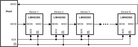 Figure 9. SPI Daisy Chain System Architecture
In a daisy-chain configuration of N LMH0395 devices, the host conceptually sees a shift register of length 16xN. Therefore the length of SPI transactions (as previously described) is 16xN bits, and SS must be asserted for 16xN clock cycles for each SPI transaction.
7.5.1.5 SPI Daisy-Chain Write
Figure 10 shows the SPI daisy-chain write for a daisy-chain of N devices. The SS signal is driven low and SCK is toggled for 16xN clocks. The 16xN bit MOSI payload (sent to Device 1 in the daisy-chain) consists of the 16-bit SPI write data for Device N (the last device in the chain), followed by the write data for Device –1, Device –2, and so forth, ending with the write data for Device 1 (the first device in the chain). The 16-bit SPI write data for each device consists of a “0” (write command), seven address bits, and eight data bits. After the SPI daisy-chain write, SS must return high and then the write occurs for all devices in the daisy-chain.
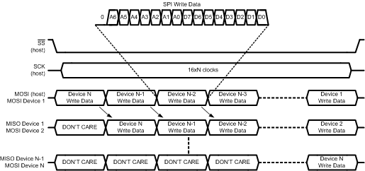 Figure 10. SPI Daisy-Chain Write
7.5.1.6 SPI Daisy-Chain Read
Figure 11 shows the SPI daisy-chain read for a daisy-chain of N devices. The SPI daisy-chain read is 32xN bits long, consisting of 16xN bits for the read transaction followed by 16xN bits for the dummy read transaction (all “1”s) to shift out the read data on the MISO output. The SS signal is driven low and SCK is toggled for 16xN clocks. The first 16xN bit MOSI payload (sent to Device 1 in the daisy-chain) consists of the 16-bit SPI read data for Device N (the last device in the chain), followed by the read data for Device –1, Device –2, and so forth, ending with the read data for Device 1 (the first device in the chain). The 16-bit SPI read data for each device consists of a “1” (read command), seven address bits, and eight “1”s (which are ignored). After the first 16xN bit transaction, SS must return high (to latch the data) and then is driven low again before the second 16xN bit transaction of all “1”s is sent to the MOSI input. The requested read data is shifted out on MISO starting with the data for Device N and ending with the data for Device 1. After this transaction, SS must return high.
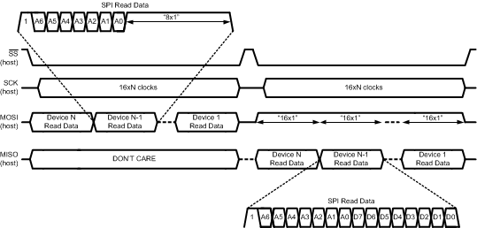 Figure 11. SPI Daisy-Chain Read
7.5.1.7 SPI Daisy-Chain Read and Write Example
The following example further clarifies LMH0395 SPI daisy-chain operation. Assume a daisy-chain of three LMH0395 devices (Device 1, Device 2, and Device 3), with Device 1 as the first device in the chain and Device 3 as the last device in the chain, as shown by the first three devices in Figure 9. Because there are three devices in the daisy-chain, each SPI transaction is 48-bits long.
This example shows an SPI operation combining SPI reads and writes in order to accomplish the following three tasks:
- Write 0x22 to register 0x01 of Device 3 in order to set the output swing of output driver 0 to 400 mVP-P.
- Read the contents of register 0x00 of Device 2.
- Write 0x10 to register 0x00 of Device 1 in order to force the sleep mode.
Figure 12 shows the two 48-bit SPI transactions required to complete these tasks (the bits are shifted in left to right).
 Figure 12. SPI Daisy-Chain Read and Write Example
The following occurs at the end of the first transaction:
- Write 0x22 to register 0x01 of Device 3.
- Latch the data from register 0x00 of Device 2.
- Write 0x10 to register 0x00 of Device 1.
In the second transaction, three dummy reads (each consisting of 16 “1”s) are shifted in, and the read data from Device 2 (with value 0x88) appears on MISO in the 25th through 32nd clock cycles.
7.5.1.8 SPI Daisy-Chain Length Detection
A useful operation for the host may be to detect the length of the daisy-chain. This is a simple matter of shifting in a series of dummy reads with a known data value (such as 0x5A). For an SPI daisy-chain of N LMH0395 devices, the known data value will appear on the host's MISO pin after N+1 writes. Assuming a daisy-chain of three LMH0395 devices, the result of this operation is shown in Figure 13.
 Figure 13. SPI Daisy-Chain Length Detection
7.5.1.9 Output Driver Adjustments and De-Emphasis Setting
The output driver swing (amplitude), offset voltage (common-mode voltage), and de-emphasis level are adjustable through SPI register 01h. The output driver to control with SPI register 01h (either output driver 0 or output driver 1) can be selected through bit 2 of SPI register 00h.
The output swing is adjustable through bits [7:6] of SPI register 01h. The default value for these register bits is 10b for a peak to peak differential output voltage of 700 mVP-P. The output swing can be set for 400 mVP-P, 600 mVP-P , 700 mVP-P, or 800 mVP-P.
The offset voltage is adjustable through bits [5:4] of SPI register 01h. The default value for these register bits is “10b” for an output offset of 1.2 V. The output common-mode voltage may be adjusted in 200 mV increments, from 0.8 V to 1.2 V. It can be set to “11b” for the maximum offset voltage. At this maximum offset voltage setting, the outputs are referenced to the positive supply and the offset voltage is around 1.35 V.
The output de-emphasis is turned on or off by bit 3 of SPI register 01h, and the de-emphasis level is set by bits [2:1] of SPI register 01h. The output de-emphasis level may be set for 0 dB (for driving up to 10” FR4), -3 dB (for driving 10-20” FR4), -5 dB (for driving 20-30” FR4), or -7 dB (for driving 30-40” FR4).
7.5.1.10 Launch Amplitude Optimization
The LMH0395 can compensate for attenuation of the input signal prior to the equalizer. This compensation is useful for applications with a passive splitter at the equalizer input or a non-ideal input termination network, and is controlled by SPI register 02h.
Bit 7 of SPI register 02h is used for the launch amplitude setting. At the default setting of “0”, the LMH0395 operates normally and expects a launch amplitude of 800 mVP-P. Bit 7 may be set to “1” to optimize the LMH0395 for input signals with 6 dB of attenuation (400 mVP-P).
7.5.1.11 Cable Length Indicator (CLI)
The cable length indicator (CLI) provides an indication of the length of the cable attached to input. CLI is accessible through bits [7:0] of SPI register 06h. The 8-bit setting ranges in decimal value from 0 to 247 (“00000000” to “11110111” binary), corresponding to 0 to 400m of Belden 1694A cable. For 3G and HD input, CLI is 1.25m per step. For SD input, CLI is 1.25m per step, less 20m, from 0 to 191 decimal, and 3.5m per step from 192 to 247 decimal.
To calculate the Belden 1694A cable length (in meters) from the CLI decimal value for 3G or HD input:
To calculate the Belden 1694A cable length (in meters) from the CLI decimal value for SD input:
FOR CLI ≤ 191,
For CLI > 191,
Figure 14 shows typical CLI values vs. Belden 1694A cable length. CLI is valid for Belden 1694A cable lengths of 0-200 m at 2.97 Gbps, 0-220 m at 1.485 Gbps, and 0-400 m at 270 Mbps. Note: Given the continuous adaptive nature of the equalizer, the CLI values may vary constantly within several steps.
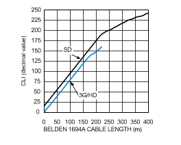 Figure 14. CLI vs. Belden 1694a Cable Length