SNLS323N August 2010 – January 2017 LMH0395
PRODUCTION DATA.
- 1 Features
- 2 Applications
- 3 Description
- 4 Revision History
- 5 Pin Configuration and Functions
- 6 Specifications
-
7 Detailed Description
- 7.1 Overview
- 7.2 Functional Block Diagram
- 7.3 Feature Description
- 7.4 Device Functional Modes
- 7.5
Programming
- 7.5.1
SPI Register Access
- 7.5.1.1 SPI Transaction Overview
- 7.5.1.2 SPI Write
- 7.5.1.3 SPI Read
- 7.5.1.4 SPI Daisy-Chain Operation
- 7.5.1.5 SPI Daisy-Chain Write
- 7.5.1.6 SPI Daisy-Chain Read
- 7.5.1.7 SPI Daisy-Chain Read and Write Example
- 7.5.1.8 SPI Daisy-Chain Length Detection
- 7.5.1.9 Output Driver Adjustments and De-Emphasis Setting
- 7.5.1.10 Launch Amplitude Optimization
- 7.5.1.11 Cable Length Indicator (CLI)
- 7.5.1
SPI Register Access
- 7.6 Register Maps
- 8 Application and Implementation
- 9 Power Supply Recommendations
- 10Layout
- 11Device and Documentation Support
- 12Mechanical, Packaging, and Orderable Information
6 Specifications
6.1 Absolute Maximum Ratings
over operating free-air temperature range (unless otherwise noted)(1)| MIN | MAX | UNIT | ||
|---|---|---|---|---|
| Supply voltage | 3.1 | V | ||
| Input voltage (all inputs) | -0.3 | VCC+0.3 | V | |
| Junction temperature | +125 | °C | ||
| Storage temperature, Tstg | -65 | +150 | °C | |
(1) Stresses beyond those listed under Absolute Maximum Ratings may cause permanent damage to the device. These are stress ratings only, which do not imply functional operation of the device at these or any other conditions beyond those indicated under Recommended Operating Conditions. Exposure to absolute-maximum-rated conditions for extended periods may affect device reliability.
6.2 ESD Ratings
| VALUE | UNIT | |||
|---|---|---|---|---|
| V(ESD) | Electrostatic discharge | Human body model (HBM), per ANSI/ESDA/JEDEC JS-001(1) | ±6000 | V |
| Charged-device model (CDM), per JEDEC specification JESD22-C101(2) | ±2000 | V | ||
(1) JEDEC document JEP155 states that 500-V HBM allows safe manufacturing with a standard ESD control process.
(2) JEDEC document JEP157 states that 250-V CDM allows safe manufacturing with a standard ESD control process.
6.3 Recommended Operating Conditions
over operating free-air temperature range (unless otherwise noted)| MIN | NOM | MAX | UNIT | |||
|---|---|---|---|---|---|---|
| VCC – VEE | Supply voltage | 2.375 | 2.5 | 2.625 | V | |
| Input coupling capacitance | 1 | µF | ||||
| TA | Operating free-air temperature | -40 | 25 | +85 | °C | |
6.4 Thermal Information
| THERMAL METRIC(1) | LMH0395 | UNIT | |
|---|---|---|---|
| RTW (WQFN) | |||
| 24 PINS | |||
| RθJA | Junction-to-ambient thermal resistance | 40 | °C/W |
| RθJC(top) | Junction-to-case (top) thermal resistance | 6 | °C/W |
(1) For more information about traditional and new thermal metrics, see the Semiconductor and IC Package Thermal Metrics application report, SPRA953.
6.5 DC Electrical Characteristics
over operating free-air temperature range (unless otherwise noted).(1)(2)(3)(4)(5)| PARAMETER | TEST CONDITIONS | MIN | TYP | MAX | UNIT | |
|---|---|---|---|---|---|---|
| VIH | Input voltage high level | Logic Inputs | 1.7 | VCC | V | |
| VIL | Input voltage low level | Logic Inputs | VEE | 0.7 | V | |
| VSDI | Input voltage swing | 0-m cable length(3) SDI | 720 | 800 | 880 | mVP−P |
| VCMIN | Input common-mode voltage | SDI or SDI | 1.65 | V | ||
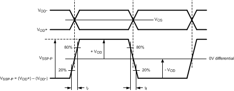
| VSSP-P | Differential output voltage, P-P | SDO0, SDO0, SDO1, SDO1 (100-Ω load), default register settings (4) , Figure 1 | 500 | 700 | 900 | mVP-P |
| VOD | Differential output voltage | 250 | 350 | 450 | mV | |
| ΔVOD | Change in magnitude of VOD for complementary output states | 50 | mV | |||
| VOS | Offset voltage | 1.1 | 1.2 | 1.35 | V | |
| ΔVOS | Change in magnitude of VOS for complementary output states | 50 | mV | |||
| IOS | Output short circuit current | 30 | mA | |||
| MUTEREF | MUTEREF DC voltage (floating) | 1.3 | V | |||
| MUTERNG | MUTEREF range | 0.8 | V | |||
| VOH | Output voltage high level | CD, MISO, IOH = –2 mA | 2 | V | ||
| VOL | Output voltage low level | CD, MISO, IOL = +2 mA | 0.2 | V | ||
| ICC | Supply current | Normal operation, dual outputs(5) | 55 | 78 | mA | |
| Normal operation, single output(5) | 45 | 65 | mA | |||
| Power-save mode | 7 | 10 | mA | |||
(1) Current flow into device pins is defined as positive. Current flow out of device pins is defined as negative. All voltages are stated referenced to VEE = 0 Volts.
(2) Typical values are stated for VCC = +2.5 V and TA = +25°C.
(3) The LMH0395 can be optimized for different launch amplitudes through the SPI.
(4) The differential output voltage and offset voltage are adjustable through the SPI.
(5) Typical ICC is measured with a 2.97-Gbps input signal.
6.6 AC Electrical Characteristics
over supply voltage and operating temperature ranges, unless otherwise specified(1).| PARAMETER | TEST CONDITIONS | MIN | TYP | MAX | UNIT | |
|---|---|---|---|---|---|---|
| BRMIN | Minimum input data rate (SDI, SDI) | 125 | Mbps | |||
| BRMAX | Maximum input data rate (SDI, SDI) | 2970 | Mbps | |||
| TJRAW | Jitter for various cable lengths | 2.97 Gbps, Belden 1694A, 0-100 meters(4)(6) |
0.2 | UI | ||
| 2.97 Gbps, Belden 1694A, 100-140 meters(4)(6) | 0.3 | UI | ||||
| 2.97 Gbps, Belden 1694A, 140-180 meters(4)(6) | 0.5 | UI | ||||
| 2.97 Gbps, Belden 1694A, 180-200 meters | 0.55 | UI | ||||
| 1.485 Gbps, Belden 1694A, 0-200 meters(4)(6) | 0.2 | UI | ||||
| 1.485 Gbps, Belden 1694A, 200-220 meters | 0.3 | UI | ||||
| 270 Mbps, Belden 1694A, 0-400 meters(4)(6) |
0.3 | UI | ||||
| tr, tf | Output rise time, fall time (SDO0, SDO0, SDO1, SDO1) | 20% – 80%, 100-Ω load, Figure 1(2) | 90 | 130 | ps | |
| ΔTR-F | Mismatch in rise/fall time (SDO0, SDO0, SDO1, SDO1) | SDO0, SDO0, SDO1, SDO1See(2) | 2 | 15 | ps | |
| tOS | Output overshoot (SDO0, SDO0, SDO1, SDO1) | 1% | 5% | |||
| RLIN | Input return loss (SDI, SDI) | 5 MHz - 1.5 GHz(5) | 15 | dB | ||
| 1.5 GHz - 3.0 GHz(5) | 10 | dB | ||||
| RIN | Input resistance (SDI, SDI,) | Single-ended | 1.5 | kΩ | ||
| CIN | Input capacitance (SDI, SDI) | Single-ended | 0.7 | pF | ||
6.7 Switching Characteristics for SPI Interface
over supply voltage and operating temperature ranges, unless otherwise specified (1).| PARAMETER | TEST CONDITIONS | MIN | TYP | MAX | UNIT | |
|---|---|---|---|---|---|---|
| tODZ | MISO driven-to-tristate time | MISO, see Figure 3 | 20 | ns | ||
| tOZD | MISO tristate-to-driven time | 10 | ns | |||
| tOD | MISO output delay time | 15 | ns | |||
(1) Typical values are stated for VCC = +2.5 V and TA = +25°C.
6.8 Timing Requirements for SPI Interface
over supply voltage and operating temperature ranges, unless otherwise specified (1).| TEST CONDITIONS | MIN | NOM | MAX | UNIT | ||
|---|---|---|---|---|---|---|
| fSCK | Frequency | SCK | 20 | MHz | ||
| tPH | SCK pulse width high | SCK, see Figure 2, Figure 3 | 40 | % SCK period | ||
| tPL | SCK pulse width low | 40 | % SCK period | |||
| tSU | MOSI set-up time | MOSI, see Figure 2, Figure 3 | 4 | ns | ||
| tH | MOSI hold time | 4 | ns | |||
| tSSSU | SS set-up time | SS, see Figure 2, Figure 3 | 14 | ns | ||
| tSSH | SS hold time | 4 | ns | |||
| tSSOF | SS OFF-time | 1 | SCK period | |||
(1) Typical values are stated for VCC = +2.5 V and TA = +25°C.
(2) Specification is ensured by characterization.
(3) The LMH0395 can be optimized for different launch amplitudes through the SPI.
(4) Based on design and characterization data over the full range of recommended operating conditions of the device. Jitter is measured in accordance with ST RP 184, ST RP 192, and the applicable serial data transmission standard: ST 424, ST 292, or ST 259.
(5) Input return loss is dependent on board design. The LMH0395 exceeds this specification on the SD395EVK evaluation board with a return loss network consisting of a 5.6-nH inductor in parallel with a 75-Ω series resistor on the input.
(6) Due to SMPTE naming convention, all SMPTE Engineering Documents will be numbered as a two-letter prefix and a number. Documents and references with the same root number and year are functionally identical; for example ST 424-2006 and SMPTE 424M-2006 refer to the same document.
 Figure 1. LVDS Output Voltage, Offset, and Timing Parameters
 Figure 2. SPI Write
 Figure 3. SPI Read
6.9 Typical Characteristics

