SNWS022D January   2010  – June 2015 LMH2110

PRODUCTION DATA.  

  1. Features
  2. Applications
  3. Description
  4. Revision History
  5. Pin Configuration and Functions
  6. Specifications
    1. 6.1 Absolute Maximum Ratings
    2. 6.2 ESD Ratings
    3. 6.3 Recommended Operating Conditions
    4. 6.4 Thermal Information
    5. 6.5 2.7-V and 4.5-V DC and AC Electrical Characteristics
    6. 6.6 Timing Requirements
    7. 6.7 Typical Characteristics
  7. Detailed Description
    1. 7.1 Overview
    2. 7.2 Functional Block Diagram
    3. 7.3 Feature Description
      1. 7.3.1 Accurate Power Measurement
      2. 7.3.2 Types of RF Detectors
        1. 7.3.2.1 Peak Detectors
        2. 7.3.2.2 LOG Amp Detectors
        3. 7.3.2.3 RMS Detectors
      3. 7.3.3 LMH2110 RF Power Detector
        1. 7.3.3.1 RF Input
        2. 7.3.3.2 Enable
        3. 7.3.3.3 Output
        4. 7.3.3.4 Supply
    4. 7.4 Device Functional Modes
  8. Application and Implementation
    1. 8.1 Application Information
    2. 8.2 Typical Applications
      1. 8.2.1 Application With Transmit Power Control
        1. 8.2.1.1 Design Requirements
        2. 8.2.1.2 Detailed Design Procedure
          1. 8.2.1.2.1 Specifying Detector Performance
            1. 8.2.1.2.1.1 Dynamic Range
            2. 8.2.1.2.1.2 Log Conformance Error
            3. 8.2.1.2.1.3 Variation Over Temperature Error
            4. 8.2.1.2.1.4 1-dB Step Error
            5. 8.2.1.2.1.5 10-dB Step Error
            6. 8.2.1.2.1.6 Variation Due to Modulation
        3. 8.2.1.3 Application Curves
      2. 8.2.2 Application With Resistive Divider
      3. 8.2.3 Application With Low-Pass Output Filter for Residual Ripple Reduction
  9. Power Supply Recommendations
  10. 10Layout
    1. 10.1 Layout Guidelines
    2. 10.2 Layout Example
  11. 11Device and Documentation Support
    1. 11.1 Community Resources
    2. 11.2 Trademarks
    3. 11.3 Electrostatic Discharge Caution
    4. 11.4 Glossary
  12. 12Mechanical, Packaging, and Orderable Information

封装选项

机械数据 (封装 | 引脚)
散热焊盘机械数据 (封装 | 引脚)
订购信息

10 Layout

10.1 Layout Guidelines

As with any other RF device, pay close careful attention to the board layout. If the board layout is not properly designed, performance might be less then can be expected for the application.

The LMH2110 is designed to be used in RF applications, having a characteristic impedance of 50 Ω. To achieve this impedance, the input of the LMH2110 needs to be connected via a 50-Ω transmission line. Transmission lines can be created on PCBs using microstrip or (grounded) coplanar waveguide (GCPW) configurations.

In order to minimize injection of RF interference into the LMH2110 through the supply lines, the PCB traces for VDD and GND must be minimized for RF signals. This can be done by placing a small decoupling capacitor between the VDD and GND. It must be placed as close as possible to the VDD and GND pins of the LMH2110.

10.2 Layout Example
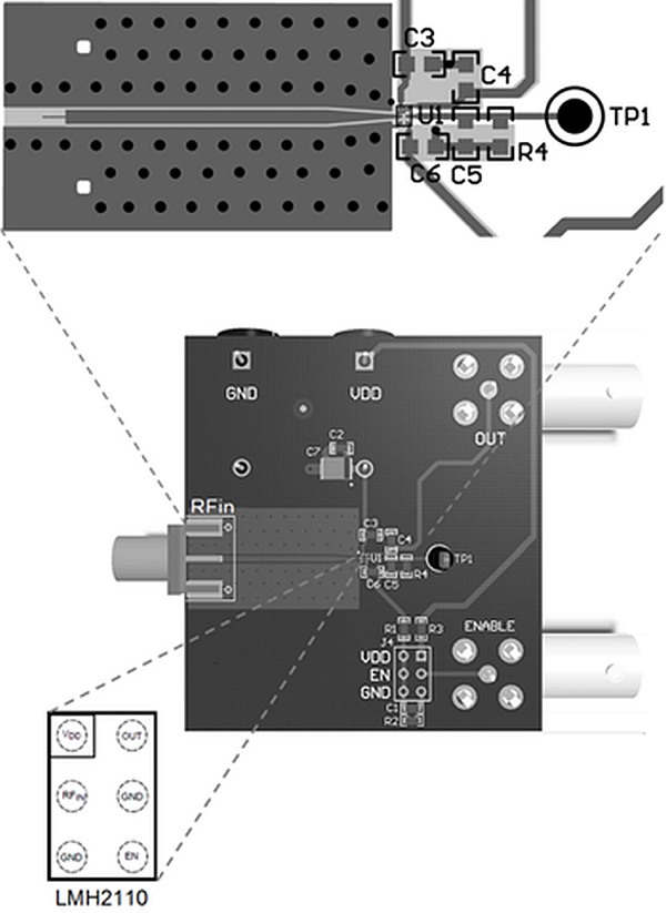
LMH2110 layout_LMH2110.pngFigure 56. LMH2110 Layout