ZHCSF77A July 2016 – July 2016 LMH2832
PRODUCTION DATA.
- 1 特性
- 2 应用
- 3 说明
- 4 修订历史记录
- 5 Device Comparison Table
- 6 Pin Configuration and Functions
- 7 Specifications
- 8 Parameter Measurement Information
- 9 Detailed Description
- 10Application and Implementation
- 11Power Supply Recommendations
- 12Layout
- 13器件和文档支持
- 14机械、封装和可订购信息
10 Application and Implementation
NOTE
Information in the following applications sections is not part of the TI component specification, and TI does not warrant its accuracy or completeness. TI’s customers are responsible for determining suitability of components for their purposes. Customers should validate and test their design implementation to confirm system functionality.
10.1 Application Information
The LMH2832 is designed as a general-purpose, analog-to-digital converter (ADC) driver that also meets the performance requirements for DOCSIS 3.X upstream CMTS solutions. This section describes various requirements and considerations for using the LMH2832 and also some design examples.
10.1.1 Driving ADCs
When the amplifier is driving an ADC, the key points to consider for implementation are the signal-to-noise ratio (SNR), spurious-free dynamic range (SFDR), and ADC input considerations, as described in this section.
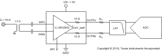
A typical application of the LMH2832 involves driving a wideband, 14-bit ADC (such as the ADS54J40), as shown in Figure 58. The LMH2832 can drive the full Nyquist bandwidth of ADCs with sampling rates up to 900 MSPS. If the front-end bandwidth of the ADC is more than 450 MHz, then use a simple noise filter to improve SNR. Otherwise, the ADC can be connected directly to the amplifier output pins with appropriate matching resistors to limit the full-scale input of the ADC. Note that the LMH2832 inputs must be driven differentially using a balun or fully differential amplifiers (FDAs). For dc-coupled applications, an FDA (such as the LMH3401 or LMH5401) that can convert a single-ended input to a differential output with low distortion is preferred.
 Figure 58. ADC Driver with a 50-Ω Source
10.1.1.1 SNR Considerations
When using the LMH2832 with a filter, the signal-to-noise ratio (SNR) of the amplifier and filter can be calculated from the amplitude of the signal and the bandwidth of the filter. The noise from the amplifier is band-limited by the filter with the equivalent brick-wall filter bandwidth. The amplifier and filter noise can be calculated using Equation 3:

where
- eFILTEROUT = eNAMPOUT • √ENB
- eNAMPOUT = the output noise density of the LMH2832 (50.4 nV/√Hz) at AV = 30 dB
- ENB = the brick-wall equivalent noise bandwidth of the filter
- VO = the amplifier output signal
For example, with a first-order (N = 1) band-pass or low-pass filter with a 1000-MHz cutoff, ENB is 1.57 • f–3dB = 1.57 • 1000 MHz = 1570 MHz. For second-order (N = 2) filters, ENB is 1.22 • f–3dB. When the filter order increases, ENB approaches f–3dB (N = 3 → ENB = 1.15 • f–3dB; N = 4 → ENB = 1.13 • f–3dB). Both VO and eFILTEROUT are in RMS voltages. For example, with a 2-VPP (0.707 VRMS) output signal and a 300-MHz, first-order, low-pass filter, the SNR of the amplifier and filter is 56 dB with eFILTEROUT = 50.4 nV/√Hz • √471 MHz = 1.09 mVRMS.
The SNR of the amplifier, filter, and ADC sum in RMS fashion, as shown in Equation 4 (SNR values in dB):

This formula shows that if the SNR of the amplifier and filter equals the SNR of the ADC, then the combined SNR is 3 dB lower (worse). Thus, for minimal degradation (< 1 dB) on the ADC SNR, the SNR of the amplifier and filter must be 10 dB greater than the ADC SNR. The combined SNR calculated in this manner is usually accurate to within ±1 dB of the actual implementation.
10.1.1.2 SFDR Considerations
The SFDR of the amplifier is usually set by the second- or third-order harmonic distortion for single-tone inputs, and by the second-order or third-order intermodulation distortion for two-tone inputs. Harmonics and second-order intermodulation distortion can be filtered to some degree, but third-order intermodulation spurs cannot be filtered. The ADC generates the same distortion products as the amplifier, but also generates additional spurs (not harmonically related to the input signal) as a result of sampling and clock feed through.
When the spurs from the amplifier and filter are known, each individual spur can be directly added to the same spur from the ADC, as shown in Equation 5, to estimate the combined spur (spur amplitudes in dBc):

This calculation assumes that the spurs are in phase, but usually provides a good estimate of the final combined distortion.
For example, if the spur of the amplifier and filter equals the spur of the ADC, then the combined spur is 6 dB higher. To minimize the amplifier contribution (< 1 dB) to the overall system distortion, the spur from the amplifier and filter must be approximately 15 dB lower in amplitude than that of the converter. The combined spur calculated in this manner is usually accurate to within ±6 dB of the actual implementation; however, higher variations can be detected as a result of phase shift in the filter, especially in second-order harmonic performance.
This worst-case spur calculation assumes that the amplifier and filter spur of interest is in phase with the corresponding spur in the ADC, such that the two spur amplitudes can be added linearly. There are two phase-shift mechanisms that cause the measured distortion performance of the amplifier-ADC chain to deviate from the expected performance calculated using Equation 5; one mechanism is the common-mode phase shift and the other is the differential phase shift.
Common-mode phase shift is the phase shift detected equally in both branches of the differential signal path including the filter. Common-mode phase shift nullifies the basic assumption that the amplifier, filter, and ADC spur sources are in phase. This phase shift can lead to better performance than predicted when the spurs become phase shifted, and there is the potential for cancellation when the phase shift reaches 180°. However, there is a significant challenge in designing an amplifier-ADC interface circuit to take advantage of a common-mode phase shift for cancellation: the phase characteristics of the ADC spur sources are unknown, thus the necessary phase shift in the filter and signal path for cancellation is also unknown.
Differential phase shift is the difference in the phase response between the two branches of the differential filter signal path. Differential phase shift in the filter is a result of mismatched components caused by nominal tolerances and can severely degrade the even harmonic distortion of the amplifier-ADC chain. This effect has the same result as mismatched path lengths for the two differential traces, and causes more phase shift in one path than the other. Ideally, the phase responses over frequency through the two sides of a differential signal path are identical, such that even harmonics remain optimally out of phase and cancel when the signal is taken differentially. However, if one side has more phase shift than the other, then the even harmonic cancellation is not as effective.
Single-order, resistor-capacitor (RC) filters cause very little differential phase shift with nominal tolerances of 5% or less, but higher-order, inductor-capacitor (LC) filters are very sensitive to component mismatch. For instance, a third-order Butterworth band-pass filter with a 100-MHz center frequency and a 20-MHz bandwidth displays as much as 20° of differential phase imbalance in a SPICE Monte Carlo analysis with 2% component tolerances. Therefore, although a prototype may work, production variance is unacceptable. For ac-coupled or dc-coupled applications where a transformer or balun cannot be used, using first- or second-order filters is recommended to minimize the effect of differential phase shift.
10.1.1.3 ADC Input Common-Mode Voltage Considerations (AC-Coupled Input)
When interfacing to an ADC, the input common-mode voltage range of the ADC must be taken into account for proper operation. In an ac-coupled application between the amplifier and the ADC, the input common-mode voltage bias of the ADC can be accomplished in different ways. Some ADCs use internal bias networks such that the analog inputs are automatically biased to the required input common-mode voltage if the inputs are ac-coupled with capacitors (or if the filter between the amplifier and ADC is a band-pass filter). Other ADCs supply the required input common-mode voltage from a reference voltage output pin (often termed CM or VCM). With these ADCs, the ac-coupled input signal can be re-biased to the input common-mode voltage by connecting resistors from each input to the CM output of the ADC, as shown in Figure 59. AC coupling provides dc common-mode isolation between the amplifier and the ADC; thus, the output common-mode voltage of the amplifier is a don’t care for the ADC.
 Figure 59. Biasing AC-Coupled ADC Inputs Using the ADC CM Output
10.1.1.4 ADC Input Common-Mode Voltage Considerations (DC-Coupled Input)
The LMH2832 is designed to primarily be used in ac-coupled applications only. However, the LMH2832 can be dc-coupled if certain strict conditions are met. The LMH2832 has an internal common-mode bias equal to the mid-supply voltage, so any dc coupling on the input or output must have a common-mode voltage that is also set to mid-supply. To dc couple to an ADC input, the mid-supply voltage of the LMH2832 must be centered around the ADC input common-mode. This common-mode matching can be accomplished by shifting the supplies to center the mid-supply voltage around the ADC input common-mode voltage. However, shifting the supplies also changes the ground reference for the digital inputs, which then likely requires a voltage-shifted interface as well. The LMH2832 is not recommended to be operated as dc-coupled unless absolutely necessary.
10.2 Typical Applications
10.2.1 DOCSIS 3.X Driver
The LMH2832 is designed to perform best when driving differential input ADCs in high-speed applications. Figure 60 shows an example diagram of the LMH2832 driving an ADC with a fifth-order, low-pass filter for a 75-Ω impedance, data over cable service interface specification (DOCSIS) 3.X upstream receiver return path application. The primary interface between the amplifier and the ADC is usually an antialiasing filter to suppress high-frequency harmonics that otherwise alias back into the ADC FFT spectrum. Filters range from single-order real RC poles to higher-order, resistor-inductor-capacitor (RLC) filters, depending on the application requirements. Series output resistors (RO) help isolate the amplifier from any capacitive load presented by the filter, and can also be used to create a matched impedance to drive transmission lines.
 Figure 60. DOCSIS 3.X Driver with the ADS54J40 and a 300-MHz, 4th-Order, Butterworth, Low-Pass Filter
10.2.1.1 Design Requirements
Table 12 shows example design requirements for the LMH2832 in an upstream receiver application.
Table 12. Example Design Requirements
| SPECIFICATION | DESIGN REQUIREMENTS |
|---|---|
| Supply voltage | 4.75 to 5.25 V |
| Usable input frequency range | 300 MHz |
| System voltage gain and range | 33-dB voltage gain with 30-dB range |
| Source impedance | 75 Ω, single-ended |
| Signal path SNR at 175 MHz (measured at ADC) | > 50 dBFS |
10.2.1.2 Detailed Design Procedure
To begin the design process, make sure that none of the following design parameters exceed the limits listed in the Electrical Characteristics table, such as:
- Supply voltage
- Temperature range
- Input voltage range across gain
- Output current requirements
- Digital I/O voltages and currents
10.2.1.2.1 Source Resistance Matching
Standard DOCSIS systems use a characteristic single-ended impedance of 75 Ω that must be properly matched to the 150-Ω differential impedance of the LMH2832. The circuit in Figure 60 uses a transformer with a 1:2-Ω ratio to convert the signal from single-ended to differential, and also to match the differential impedance. The transformer also adds a signal gain of approximately 3 dB to the system with some insertion loss depending on the chosen transformer.
10.2.1.2.2 Output Impedance Matching
For the circuit in Figure 60, the output impedance is matched to a 150-Ω characteristic impedance filter to maximize the performance of the LMH2832. On the amplifier output side, the output impedance is matched to 150 Ω by including a 65-Ω series resistor on each output. Combined with the internal 10-Ω resistors on each output, the total differential impedance becomes 150 Ω. The ADS54J40 has an input impedance of approximately 600 Ω that is reduced to 150 Ω by using two 5-Ω series input resistors in parallel with two 100-Ω series resistors. The 5-Ω series resistors are included to isolate the input capacitance of the ADC so that the response of the filter is not affected. With both the amplifier and ADC impedances matched, any transmission line effects of the connection are minimized.
If the ADC is physically located close enough to the amplifier, a matched impedance may not be needed; see Driving Low Insertion-Loss Filters section for more information on driving non-matched filters.
10.2.1.2.3 Voltage Headroom Considerations
Because of the series resistors included on both the amplifier outputs and ADC inputs, the amplifier must drive a voltage that is significantly higher than the ADC full-scale input. For the circuit in Figure 60, the ADS54J40 full-scale input voltage is 1.9 VPP, so the required voltage at the amplifier output pins is 3.6 VPP. This voltage is less than the specified output voltage of 5 VPP for the LMH2832, thus system performance is not limited. If the required output voltage is higher than what the amplifier can support, then the matched resistance value can be reduced. However, this reduction can have performance implications because more current output is required from the amplifier.
The input voltage swing can be larger than the output voltage swing because the LMH2832 can operate as an attenuator. To maintain the full-scale voltage of the ADS54J40 input in this application, the amplifier cannot attenuate more than 1 dB from input to output; otherwise, the maximum input voltage swing is exceeded. If the amplifier must be operated with more attenuation, then the output voltage must be reduced.
10.2.1.3 Application Curve
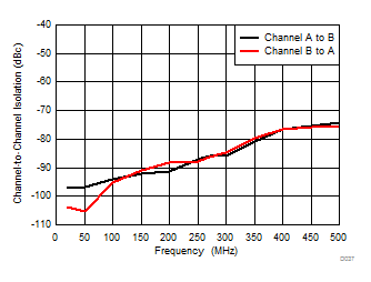
 Figure 61. Amplifier Dual Channel Isolation Presented to ADC Interface
10.2.2 IQ Receiver
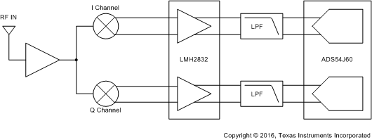
The LMH2832 is a dual-channel device; therefore, the device has excellent gain and phase matching between channels A and B. This matching makes the LMH2832 an excellent choice for systems that require two matched channels (such as an IQ demodulation receiver), as shown in Figure 62. For an IQ system, both the gain and phase must match for the real and imaginary channel. When using two single-channel amplifiers, the matching characteristics are subject to process lot and packaging variations for two individual devices, and there is often no way to make sure that the amplifiers match without testing each amplifier. However, the dual-channel architecture of the LMH2832 allows for much tighter gain and phase matching with minimal crosstalk effects. For more matching information, see the Electrical Characteristics table.
 Figure 62. IQ Receiver Block Diagram
10.3 Do's and Don'ts
10.3.1 Do:
- Include a thermal analysis at the beginning of the project
- Use well-terminated transmission lines for all signals
- Maintain symmetrical input and output trace layouts
- Use solid metal layers for the power supplies
- Keep signal lines as straight as possible
10.3.2 Don't:
- Use a lower power-supply voltage than necessary
- Forget about the common-mode response of filters and transmission lines
- Rout digital line traces close to the analog signals and supply line traces