ZHCSF77A July 2016 – July 2016 LMH2832
PRODUCTION DATA.
- 1 特性
- 2 应用
- 3 说明
- 4 修订历史记录
- 5 Device Comparison Table
- 6 Pin Configuration and Functions
- 7 Specifications
- 8 Parameter Measurement Information
- 9 Detailed Description
- 10Application and Implementation
- 11Power Supply Recommendations
- 12Layout
- 13器件和文档支持
- 14机械、封装和可订购信息
7 Specifications
7.1 Absolute Maximum Ratings
over operating free-air temperature range (unless otherwise noted)(1)| MIN | MAX | UNIT | ||
|---|---|---|---|---|
| Power supply | –0.5 | 5.5 | V | |
| Input applied to analog inputs | INPA, INMA, INPB, INMB | –0.5 | 5.5 | V |
| Voltage applied to input pins | –0.5 | 5.5 | V | |
| Digital input/output voltage range | –0.3 | 2 | V | |
| Operating junction temperature, TJ | 125 | °C | ||
| Storage temperature, Tstg | –40 | 125 | °C | |
(1) Stresses beyond those listed under Absolute Maximum Ratings may cause permanent damage to the device. These are stress ratings only, which do not imply functional operation of the device at these or any other conditions beyond those indicated under Recommended Operating Conditions. Exposure to absolute-maximum-rated conditions for extended periods may affect device reliability.
7.2 ESD Ratings
| VALUE | UNIT | |||
|---|---|---|---|---|
| V(ESD) | Electrostatic discharge | Human body model (HBM), per ANSI/ESDA/JEDEC JS-001(1) | ±2000 | V |
| Charged device model (CDM), per JEDEC specification JESD22-C101(2) | ±1000 | |||
(1) JEDEC document JEP155 states that 500-V HBM allows safe manufacturing with a standard ESD control process.
(2) JEDEC document JEP157 states that 250-V CDM allows safe manufacturing with a standard ESD control process.
7.3 Recommended Operating Conditions
over operating free-air temperature range (unless otherwise noted)| MIN | NOM | MAX | UNIT | ||
|---|---|---|---|---|---|
| VS | Power-supply voltage | 4.75 | 5 | 5.25 | V |
| Specified operating temperature range | –40 | 85 | °C | ||
7.4 Thermal Information
| THERMAL METRIC(1) | LMH2832 | UNIT | |
|---|---|---|---|
| RHA (VQFN) | |||
| 40 PINS | |||
| RθJA | Junction-to-ambient thermal resistance | 29.5 | °C/W |
| RθJC(top) | Junction-to-case (top) thermal resistance | 20.4 | °C/W |
| RθJB | Junction-to-board thermal resistance | 6.6 | °C/W |
| ψJT | Junction-to-top characterization parameter | 0.3 | °C/W |
| ψJB | Junction-to-board characterization parameter | 6.5 | °C/W |
| RθJC(bot) | Junction-to-case (bottom) thermal resistance | 2.3 | °C/W |
(1) For more information about traditional and new thermal metrics, see the Semiconductor and IC Package Thermal Metrics application report (SPRA953).
7.5 Electrical Characteristics
at TA = 25°C, VS+ = 5 V, Ri = 75 Ω, RL = 150 Ω, maximum gain (1:2-Ω ratio transformer plus 30-dB DVGA gain), f = 5 MHz to 300 MHz, VO converted to single-ended (SE) measurement with a transformer, and default current setting (unless otherwise noted); upon power-up, gain is set to mid-range| PARAMETER | TEST CONDITIONS | MIN | TYP | MAX | UNIT | TEST LEVEL(4) | |
|---|---|---|---|---|---|---|---|
| AC PERFORMANCE | |||||||
| LSBW | Large-signal, –3-dB bandwidth |
G = 30 dB, VO = 2 VPP | 1140 | MHz | C | ||
| G = 0 dB, VO = 2 VPP | 2350 | C | |||||
| BW | Bandwidth for 0.1-dB flatness | 300 | MHz | C | |||
| HD2 | Second-order harmonic distortion | f = 100 MHz, VO = 2 VPP | –88 | dBc | C | ||
| f = 200 MHz, VO = 2 VPP | –76 | C | |||||
| f = 300 MHz, VO = 2 VPP | –63 | C | |||||
| f = 450 MHz, VO = 2 VPP | –58 | C | |||||
| HD3 | Third-order harmonic distortion | f = 100 MHz, VO = 2 VPP | –94 | dBc | C | ||
| f = 200 MHz, VO = 2 VPP | –90 | C | |||||
| f = 300 MHz, VO = 2 VPP | –81 | C | |||||
| f = 450 MHz, VO = 2 VPP | –75 | C | |||||
| IMD3 | Third-order intermodulation distortion | f = 100 MHz, tone spacing = 2 MHz, POUT(1) = 0 dBm per tone | –106 | dBc | C | ||
| f = 200 MHz, tone spacing = 2 MHz | –102 | C | |||||
| f = 300 MHz, tone spacing = 2 MHz | –86 | C | |||||
| OIP3 | Output third-order intercept point | f = 100 MHz, tone spacing = 2 MHz, POUT = 0 dBm per tone |
53 | dBm | C | ||
| f = 200 MHz, tone spacing = 2 MHz, POUT = 0 dBm per tone |
51 | C | |||||
| f = 300 MHz, tone spacing = 2 MHz, POUT = 0 dBm per tone |
43 | C | |||||
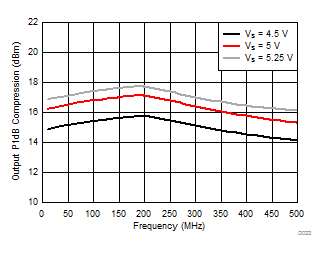
| P1dB | 1-dB compression point | f = 100 MHz, RL = 150 Ω | 16 | dBm | C | ||
| f = 200 MHz, RL = 150 Ω | 16 | C | |||||
| f = 300 MHz, RL = 150 Ω | 16.5 | C | |||||
| NF | Noise figure | Ri = 150 Ω, f = 300 MHz, max gain | 6.5 | dB | C | ||
| Output-referred voltage noise | f = 300 MHz, max gain | 47.7 | nV/√Hz | C | |||
| S11 | Input return loss | f = 300 MHz | 17 | dB | C | ||
| S22 | Reverse Isolation | Including input transformer, f < 300 MHz | 53 | dB | C | ||
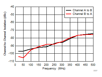
| Channel-to-channel crosstalk | f = 300 MHz, channel A to B | –77 | dB | C | |||
| f = 300 MHz, channel B to A | –81 | ||||||
| Channel-to-channel phase matching | f = 200 MHz | ±0.1 | ° | C | |||
| Channel-to-channel gain matching | f = 200 MHz | ±0.05 | dB | C | |||
| GAIN PARAMETERS | |||||||
| Maximum voltage gain | f = dc, gain code = 00h | 29.5 | 30 | 30.5 | dB | A | |
| Minimum voltage gain | f = dc, gain code = 27h | –9.5 | –9 | –8.5 | dB | A | |
| Gain range | 39 | dB | C | ||||
| Gain step size | Between any two adjacent gain settings | 0.75 | 1 | 1.25 | dB | A | |
| EG | Gain error | For any gain value | –0.5 | 0 | 0.5 | dB | A |
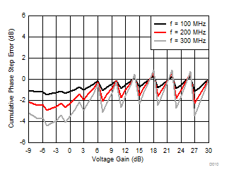
| Cumulative gain error | Referenced to max gain | –1 | 1 | dB | A | ||
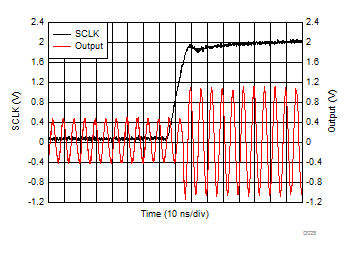
| Gain step transition time | 6 | ns | C | ||||
| ANALOG INPUT CHARACTERISTICS | |||||||
| zin | Input resistance | f = dc, differential | 135 | 150 | 165 | Ω | A |
| Cin | Input capacitance | Differential | 0.6 | pF | C | ||
| Single-ended input resistance | f = dc | 67.5 | 75 | 82.5 | Ω | A | |
| Single-ended input capacitance | 1.2 | pF | C | ||||
| VICM | Input common-mode voltage | Internally biased to mid-supply | –0.2 | 0.2 | V | A | |
| VIL | Low-level input voltage range | Differential gain shift < 1 dB | (VS–) + 1.5 | V | C | ||
| VIH | High-level input voltage range | Differential gain shift < 1 dB | (VS+) – 1.5 | V | C | ||
| ANALOG OUTPUT CHARACTERISTICS | |||||||
| zo | Output resistance | Differential | 20 | Ω | C | ||
| VOL | Low-level output voltage range | VS = 5 V, GND = 0 V | 1.15 | 1.25 | V | A | |
| VOH | High-level output voltage range | VS = 5 V, GND = 0 V | 3.75 | 3.85 | V | A | |
| VOM | Maximum output voltage swing | TA = 25°C | 5 | 5.4 | V | A | |
| TA = –40°C to +85°C | 5.4 | 6.4 | B | ||||
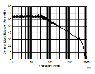
| CMRR | Common-mode rejection ratio | 56 | dB | C | |||
| POWER SUPPLY | |||||||
| VS | Supply voltage | 4.75 | 5.0 | 5.25 | V | A | |
| IQ | Quiescent current per channel | Default current, default bias setting | 102 | 105 | 108 | mA | A |
| Min current, lowest power setting | 90 | C | |||||
| Max current, highest bias setting | 108 | C | |||||
| ±PSRR | Power-supply rejection ratio(2) | Gain = 30 dB | –48 | dB | C | ||
| POWER-DOWN(3) | |||||||
| Power-down quiescent current (per channel) | TA = 25°C | 2.5 | 6 | mA | A | ||
| TA = –40°C to +85°C | 6.5 | B | |||||
| Power-down bias current | –2 | –1 | µA | A | |||
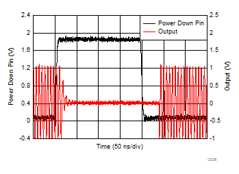
| Turn-on time delay | Time to VO = 90% of final value, gain = 0 dB, VI = 2 V |
55 | ns | C | |||
| Turn-off time delay | Time to VO = 10% of original value, gain = 0 dB, VI = 2 V |
110 | ns | C | |||
| Forward isolation in PD mode | f = 300 MHz | –67 | dB | C | |||
| DIGITAL INPUTS/OUTPUTS | |||||||
| VIH | High-level input voltage | 1.4 | 2 | V | A | ||
| VIL | Low-level input voltage | –0.3 | 0.8 | V | A | ||
| VOH | High-level output voltage | IOH = –100 µA | 1.65 | V | A | ||
| IOH = –2 mA | 1.55 | A | |||||
| VOL | Low-level output voltage | IOL = 100 µA | 0.1 | V | A | ||
| IOL = 2 mA | 0.2 | A | |||||
(1) POUT is the signal tone power at the output of the device.
(2) PSRR is defined with respect to a differential output.
(3) The device power-down function can be controlled by the PDx pins or by the power-down register accessible from the SPI interface.
(4) Test levels: (A) 100% tested at 25°C. Overtemperature limits by characterization and simulation. (B) Limits set by characterization and simulation. (C) Typical value only for information.
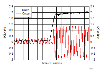
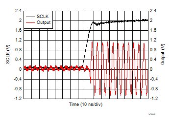
7.6 Timing Requirements: SPI
| MIN | TYP | MAX | UNIT | ||
|---|---|---|---|---|---|
| fS_C | SCLK frequency(1) | 0 | 25 | 50 | MHz |
| tPH | SCLK pulse duration, high | 10 | ns | ||
| tPL | SCLK pulse duration, low | 10 | ns | ||
| tSU | SDI setup | 3 | ns | ||
| tH | SDO hold | 3 | ns | ||
| tIZ | SDO tri-state | 3 | ns | ||
| tODZ | SDO driven to tri-state(2) | 0 | 10 | 20 | ns |
| tOZD | SDO tri-state to driven | 0 | 2 | 5 | ns |
| tOD | SDO output delay(2) | 0 | 10 | 12 | ns |
| tCSS | CS setup(3) | 3 | 5 | ns | |
| tCSH | CS hold | 3 | ns | ||
| tIAG | Inter-access gap | 20 | ns | ||
(1) Tested on the automated test equipment (ATE) only up to 25 MHz.
(2) Referenced to the negative edge of SCLK.
(3) Referenced to the positive edge of SCLK.
7.7 Typical Characteristics
at TA = 25°C, VS+ = 5 V, Ri = 75 Ω, RL = 150 Ω, maximum gain (1:2-Ω ratio transformer plus 30-dB DVGA gain), f = 5 MHz to 300 MHz, VO converted to single-ended (SE) measurement with transformer, and default current setting (unless otherwise noted); upon power-up, gain is set to mid-range
| VO = 2 VPP |
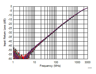
| Differential input impedance (ZIN) = 150 Ω, all gain settings |
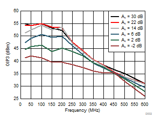
| POUT = 0 dBm per tone |
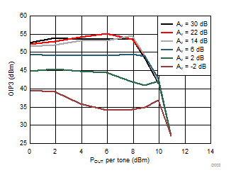
| f = 200 MHz |
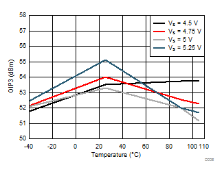
| POUT = 0 dBm per tone |
(f = 200 MHz)
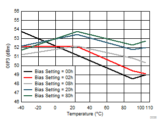
| POUT = 0 dBm per tone |
(f = 200 MHz)
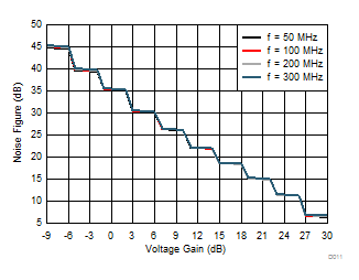
| ZIN = 150 Ω |

| VO = 2 VPP |
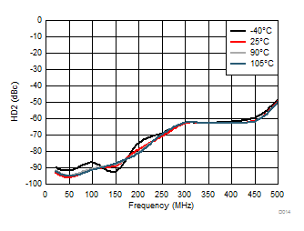
| VO = 2 VPP |
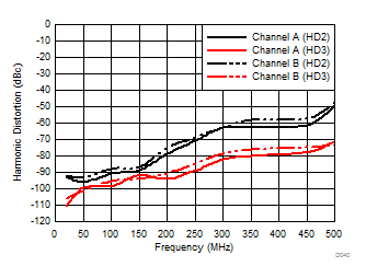
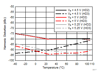
| VO = 2 VPP |
Supply Voltage (200 MHz)
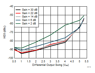
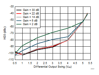
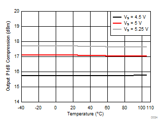
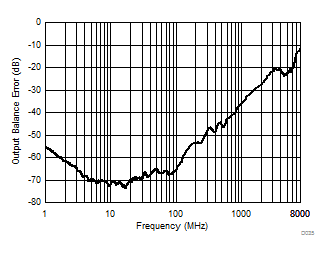
| Scd21 / Sdd21 |
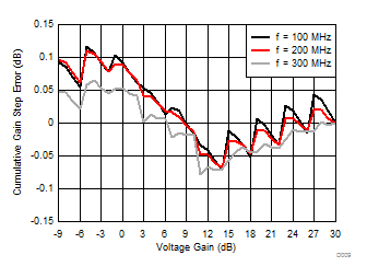
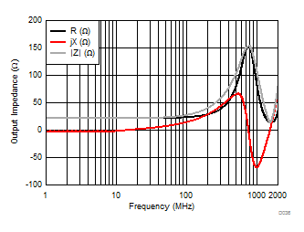
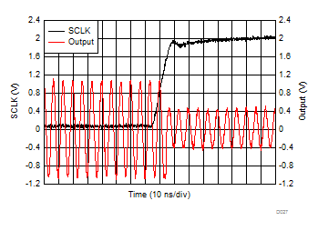
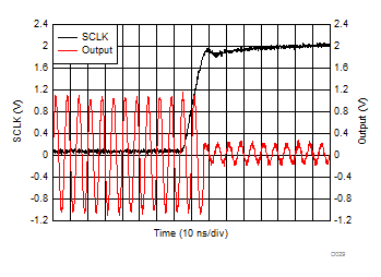
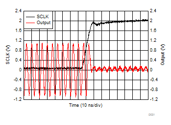
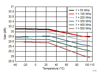
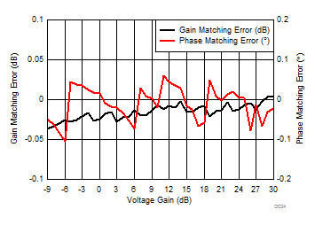
| f = 200 MHz |
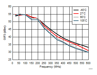
| POUT = 0 dBm per tone |
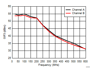
| POUT = 0 dBm per tone |
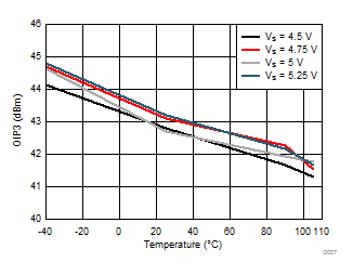
| POUT = 0 dBm per tone |
(f = 300 MHz)
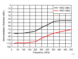
| POUT = 0 dBm per tone |
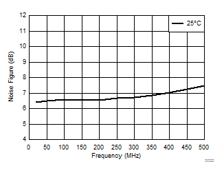
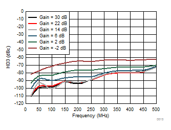
| VO = 2 VPP |
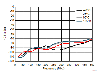
| VO = 2 VPP |
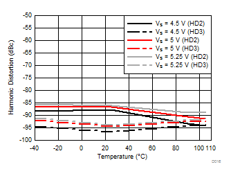
| VO = 2 VPP |
Supply Voltage (100 MHz)
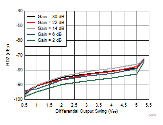
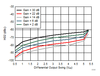
| Sdd21 / Scc21 |
