ZHCSMW3A December 2020 – November 2021 LMH32404-Q1
PRODUCTION DATA
5 Pin Configuration and Functions
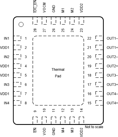
 Figure 5-1 RHF
Package, 28-Pin VQFN, Top View
Figure 5-1 RHF
Package, 28-Pin VQFN, Top ViewTable 5-1 Pin Functions
| PIN | I/O | DESCRIPTION | |
|---|---|---|---|
| NAME | NO. | ||
| EN | 9 | I | Device enable pin. EN = logic low = normal operation (default); EN = logic high = low power mode.(1) |
| GND | 11,26 | I | Amplifier ground. |
| IDC_EN | 28 | I | Ambient light cancellation loop enable. IDC_EN = logic low = enable DC cancellation (default); IDC_EN = logic high = disable DC cancellation.(1) |
| IN1 | 1 | I | Transimpedance amplifier input - Channel 1. |
| IN2 | 3 | I | Transimpedance amplifier input - Channel 2. |
| IN3 | 6 | I | Transimpedance amplifier input - Channel 3. |
| IN4 | 8 | I | Transimpedance amplifier input - Channel 4. |
| M1 | 25 | I | Select Channel 1. M1 = logic high = Channel 1 operational and output switches closed. M1 = logic low (default) = Channel 1 in standby power mode and output switches open. (1) |
| M2 | 24 | I | Select Channel 2. M2 = logic high = Channel 2 operational and output switches closed. M2 = logic low (default) = Channel 2 in standby power mode and output switches open. (1) |
| M3 | 13 | I | Select Channel 3. M3 = logic high = Channel 3 operational and output switches closed. M3 = logic low (default) = Channel 3 in standby power mode and output switches open. (1) |
| M4 | 12 | I | Select Channel 4. M4 = logic high = Channel 4 operational and output switches closed. M4 = logic low (default) = Channel 4 in standby power mode and output switches open. (1) |
| OUT1– | 22 | O | Channel 1 inverting amplifier output. When light is incident on the photodiode the output pin transitions in a negative direction from the no light condition. |
| OUT1+ | 21 | O | Channel 1 noninverting amplifier output. When light is incident on the photodiode the output pin transitions in a positive direction from the no light condition. |
| OUT2– | 20 | O | Channel 2 inverting amplifier output. When light is incident on the photodiode the output pin transitions in a negative direction from the no light condition. |
| OUT2+ | 19 | O | Channel 2 noninverting amplifier output. When light is incident on the photodiode the output pin transitions in a positive direction from the no light condition. |
| OUT3– | 18 | O | Channel 3 inverting amplifier output. When light is incident on the photodiode the output pin transitions in a negative direction from the no light condition. |
| OUT3+ | 17 | O | Channel 3 noninverting amplifier output. When light is incident on the photodiode the output pin transitions in a positive direction from the no light condition. |
| OUT4– | 16 | O | Channel 4 inverting amplifier output. When light is incident on the photodiode the output pin transitions in a negative direction from the no light condition. |
| OUT4+ | 15 | O | Channel 4 noninverting amplifier output. When light is incident on the photodiode the output pin transitions in a positive direction from the no light condition. |
| VDD1 | 2, 4, 5, 7 | I | Positive power supply for the transimpedance amplifier stage. Each pin should be tied to the same power supply with independent power-supply bypassing. |
| VDD2 | 14,23 | I | Positive power supply for the differential amplifier stage. Tie VDD1 and VDD2 to the same power supply with independent power-supply bypassing. |
| VOCM | 27 | I | Differential amplifier common-mode output control. |
| VOD | 10 | I | Differential amplifier differential output offset control. |
| Thermal pad | — | Connect the thermal pad to the same potential as pin 11 and 26 (GND). | |
(1) TI recommends driving a digital pin with a low-impedance source rather
than leaving the pin floating because fast-moving transients can couple into the pin and
inadvertently change the logic level.