ZHCSH86B December   2017  – February 2019 LMH5401-SP

PRODUCTION DATA.  

  1. 特性
  2. 应用
  3. 说明
    1.     Device Images
      1.      LMH5401-SP 小信号频率响应
      2.      LMH5401-SP 驱动 ADC12D1620QML
  4. 修订历史记录
  5. 说明 (续)
  6. Pin Configuration and Functions
    1.     Pin Functions
  7. Specifications
    1. 7.1 Absolute Maximum Ratings
    2. 7.2 ESD Ratings
    3. 7.3 Recommended Operating Conditions
    4. 7.4 Thermal Information
    5. 7.5 Electrical Characteristics: VS = 5 V
    6. 7.6 Electrical Characteristics: VS = 3.3 V
    7. 7.7 Typical Characteristics: 5 V
    8. 7.8 Typical Characteristics: 3.3 V
  8. Parameter Measurement Information
    1. 8.1  Output Reference Nodes and Gain Nomenclature
    2. 8.2  ATE Testing and DC Measurements
    3. 8.3  Frequency Response
    4. 8.4  S-Parameters
    5. 8.5  Frequency Response with Capacitive Load
    6. 8.6  Distortion
    7. 8.7  Noise Figure
    8. 8.8  Pulse Response, Slew Rate, and Overdrive Recovery
    9. 8.9  Power Down
    10. 8.10 VCM Frequency Response
    11. 8.11 Test Schematics
  9. Detailed Description
    1. 9.1 Overview
    2. 9.2 Functional Block Diagram
    3. 9.3 Feature Description
      1. 9.3.1 Fully-Differential Amplifier
      2. 9.3.2 Operations for Single-Ended to Differential Signals
        1. 9.3.2.1 AC-Coupled Signal Path Considerations for Single-Ended Input to Differential Output Conversion
        2. 9.3.2.2 DC-Coupled Input Signal Path Considerations for SE-DE Conversions
        3. 9.3.2.3 Resistor Design Equations for Single-to-Differential Applications
        4. 9.3.2.4 Input Impedance Calculations
      3. 9.3.3 Differential-to-Differential Signals
        1. 9.3.3.1 AC-Coupled, Differential-Input to Differential-Output Design Issues
        2. 9.3.3.2 DC-Coupled, Differential-Input to Differential-Output Design Issues
      4. 9.3.4 Output Common-Mode Voltage
    4. 9.4 Device Functional Modes
      1. 9.4.1 Operation With a Split Supply
      2. 9.4.2 Operation With a Single Supply
  10. 10Application and Implementation
    1. 10.1 Application Information
      1. 10.1.1 Stability, Noise Gain, and Signal Gain
      2. 10.1.2 Input and Output Headroom Considerations
      3. 10.1.3 Noise Analysis
      4. 10.1.4 Noise Figure
      5. 10.1.5 Thermal Considerations
    2. 10.2 Typical Application
      1. 10.2.1 Design Requirements
      2. 10.2.2 Detailed Design Procedure
        1. 10.2.2.1 Driving Matched Loads
        2. 10.2.2.2 Driving Unmatched Loads For Lower Loss
        3. 10.2.2.3 Driving Capacitive Loads
        4. 10.2.2.4 Driving ADCs
          1. 10.2.2.4.1 SNR Considerations
          2. 10.2.2.4.2 SFDR Considerations
          3. 10.2.2.4.3 ADC Input Common-Mode Voltage Considerations—AC-Coupled Input
          4. 10.2.2.4.4 ADC Input Common-Mode Voltage Considerations—DC-Coupled Input
        5. 10.2.2.5 GSPS ADC Driver
        6. 10.2.2.6 Common-Mode Voltage Correction
        7. 10.2.2.7 Active Balun
      3. 10.2.3 Application Curves
    3. 10.3 Do's and Don'ts
      1. 10.3.1 Do:
      2. 10.3.2 Don't:
  11. 11Power Supply Recommendations
    1. 11.1 Supply Voltage
    2. 11.2 Single Supply
    3. 11.3 Split Supply
    4. 11.4 Supply Decoupling
  12. 12Layout
    1. 12.1 Layout Guidelines
    2. 12.2 Layout Example
  13. 13器件和文档支持
    1. 13.1 器件支持
      1. 13.1.1 器件命名规则
    2. 13.2 文档支持
      1. 13.2.1 相关文档
    3. 13.3 接收文档更新通知
    4. 13.4 社区资源
    5. 13.5 商标
    6. 13.6 静电放电警告
    7. 13.7 术语表
  14. 14机械、封装和可订购信息

封装选项

机械数据 (封装 | 引脚)
散热焊盘机械数据 (封装 | 引脚)
订购信息

Typical Characteristics: 3.3 V

at TA = 25°C, VS+ = 3.3 V; VS– = 0 V; VCM = 1.65 V, RLtotal = 200-Ω differential(3) (RO = 40 Ω each), Gp = 8 dB (Gv = 17 dB), single-ended input and differential output, and input and output pins referenced to midsupply (unless otherwise noted); measured using an EVM as discussed in the section (see Figure 54 to Figure 57)
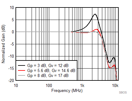
LMH5401-SP SBOS849_SEC7p7_D030_vsGAIN.gif
Figure 34. SE-DE Small Signal Frequency Response vs Gain
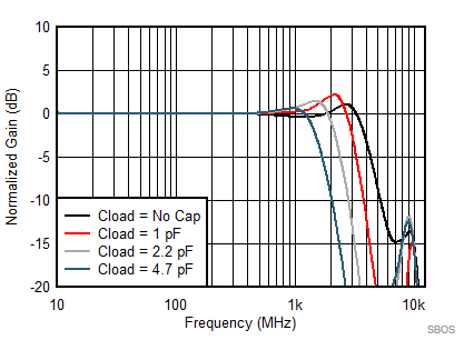
LMH5401-SP SBOS849_SEC7p7_D032_vsCLOAD.gif
Figure 36. SE-DE Small Signal Frequency Response vs Cload
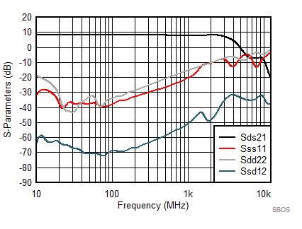
LMH5401-SP SBOS849_SEC7p7_D034_SPARAMS.gif
Figure 38. SE-DE Small Signal S-Parameters
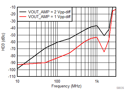
LMH5401-SP SBOS849_SEC7p7_D036_HD3vsFREQ.gif
Figure 40. SE-DE 3rd Order Harmonic Distortion vs Frequency
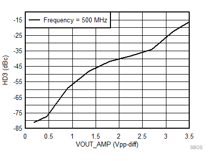
LMH5401-SP SBOS849_SEC7p7_D038_HD3vsVOUT.gif
Vout = pk-pk voltage swing per tone on 100-Ω effective load
Figure 42. SE-DE 3rd Order Harmonic Distortion vs Vout
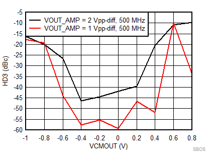
LMH5401-SP SBOS849_SEC7p7_D040_HD3vsVCMOUT.gif
Figure 44. SE-DE 3rd Order Harmonic Distortion vs Output Common Mode Voltage
LMH5401-SP SBOS849_SEC7p7_D042_HD3vsTEMP.gif
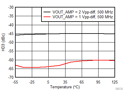
Figure 46. SE-DE 3rd Order Harmonic Distortion vs Temperature
LMH5401-SP SBOS849_SEC7p7_D044_IMD3vsFREQ.gif
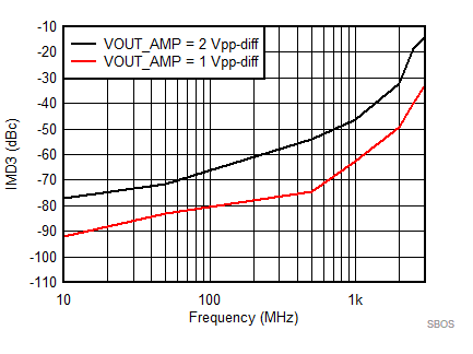
Figure 48. SE-DE 3rd Order Intermodulation Distortion vs Frequency
LMH5401-SP SBOS849_SEC7p7_D048_IMD3vsFREQ.gif
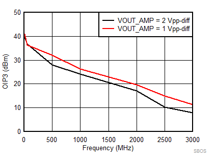
Figure 50. SE-DE Output 3rd Order Intercept Point
LMH5401-SP TC_C047_Pulse_3p3V_CM_sbos849.gif
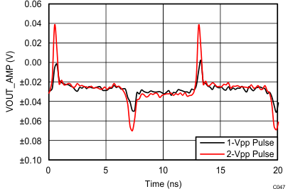
VCM @ AMPOUT Node; VCM = (Vo+ + Vo–) / 2
Figure 52. SE-DE Output Common Mode Pulse Response
LMH5401-SP SBOS849_SEC7p7_D031_vsRLOAD.gif
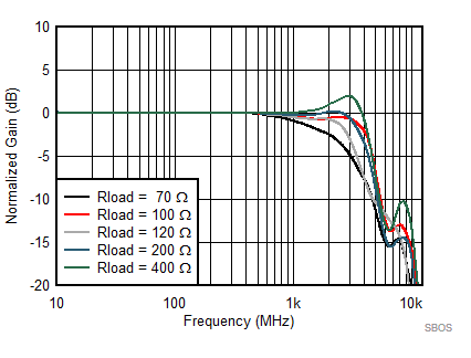
Figure 35. SE-DE Small Signal Frequency Response vs Rload
LMH5401-SP SBOS849_SEC7p7_D033_vsTEMP.gif
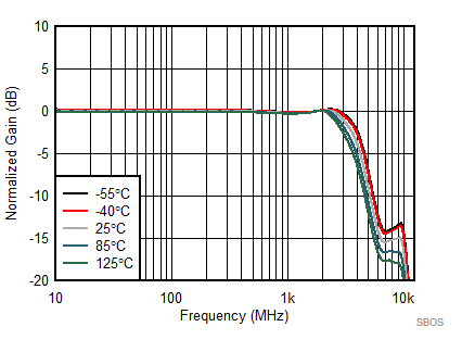
Figure 37. SE-DE Small Signal Frequency Response vs Temperature
LMH5401-SP SBOS849_SEC7p7_D035_HD2vsFREQ.gif
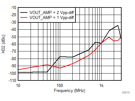
Figure 39. SE-DE 2nd Order Harmonic Distortion vs Frequency
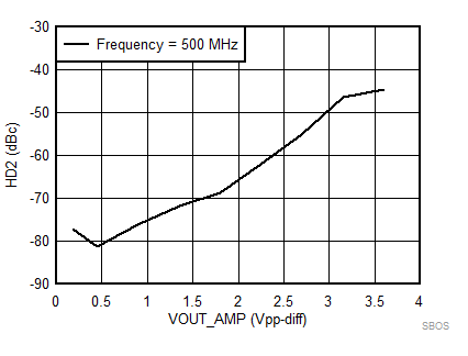
LMH5401-SP SBOS849_SEC7p7_D037_HD2vsVOUT.gif
Vout = pk-pk voltage swing per tone on 100-Ω effective load
Figure 41. SE-DE 2nd Order Harmonic Distortion vs Vout
LMH5401-SP SBOS849_SEC7p7_D039_HD2vsVCMOUT.gif
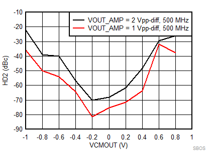
Figure 43. SE-DE 2nd Order Harmonic Distortion vs Output Common Mode Voltage
LMH5401-SP SBOS849_SEC7p7_D041_HD2vsTEMP.gif
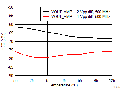
Figure 45. SE-DE 2nd Order Harmonic Distortion vs Temperature
LMH5401-SP SBOS849_SEC7p7_D043_IMD2vsFREQ.gif
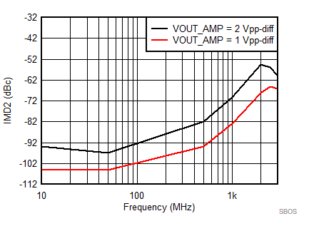
Figure 47. SE-DE 2nd Order Intermodulation Distortion vs Frequency
LMH5401-SP SBOS849_SEC7p7_D046_OIP2vsFREQ.gif
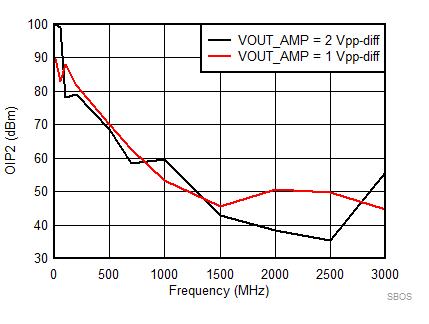
Figure 49. SE-DE Output 2nd Order Intercept Point
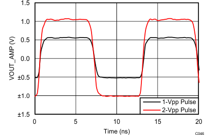
LMH5401-SP TC_C046_Pulse_3p3V_Diff_sbos849.gif
Figure 51. SE-DE Output Signal Pulse Response