ZHCSH86B December   2017  – February 2019 LMH5401-SP

PRODUCTION DATA.  

  1. 特性
  2. 应用
  3. 说明
    1.     Device Images
      1.      LMH5401-SP 小信号频率响应
      2.      LMH5401-SP 驱动 ADC12D1620QML
  4. 修订历史记录
  5. 说明 (续)
  6. Pin Configuration and Functions
    1.     Pin Functions
  7. Specifications
    1. 7.1 Absolute Maximum Ratings
    2. 7.2 ESD Ratings
    3. 7.3 Recommended Operating Conditions
    4. 7.4 Thermal Information
    5. 7.5 Electrical Characteristics: VS = 5 V
    6. 7.6 Electrical Characteristics: VS = 3.3 V
    7. 7.7 Typical Characteristics: 5 V
    8. 7.8 Typical Characteristics: 3.3 V
  8. Parameter Measurement Information
    1. 8.1  Output Reference Nodes and Gain Nomenclature
    2. 8.2  ATE Testing and DC Measurements
    3. 8.3  Frequency Response
    4. 8.4  S-Parameters
    5. 8.5  Frequency Response with Capacitive Load
    6. 8.6  Distortion
    7. 8.7  Noise Figure
    8. 8.8  Pulse Response, Slew Rate, and Overdrive Recovery
    9. 8.9  Power Down
    10. 8.10 VCM Frequency Response
    11. 8.11 Test Schematics
  9. Detailed Description
    1. 9.1 Overview
    2. 9.2 Functional Block Diagram
    3. 9.3 Feature Description
      1. 9.3.1 Fully-Differential Amplifier
      2. 9.3.2 Operations for Single-Ended to Differential Signals
        1. 9.3.2.1 AC-Coupled Signal Path Considerations for Single-Ended Input to Differential Output Conversion
        2. 9.3.2.2 DC-Coupled Input Signal Path Considerations for SE-DE Conversions
        3. 9.3.2.3 Resistor Design Equations for Single-to-Differential Applications
        4. 9.3.2.4 Input Impedance Calculations
      3. 9.3.3 Differential-to-Differential Signals
        1. 9.3.3.1 AC-Coupled, Differential-Input to Differential-Output Design Issues
        2. 9.3.3.2 DC-Coupled, Differential-Input to Differential-Output Design Issues
      4. 9.3.4 Output Common-Mode Voltage
    4. 9.4 Device Functional Modes
      1. 9.4.1 Operation With a Split Supply
      2. 9.4.2 Operation With a Single Supply
  10. 10Application and Implementation
    1. 10.1 Application Information
      1. 10.1.1 Stability, Noise Gain, and Signal Gain
      2. 10.1.2 Input and Output Headroom Considerations
      3. 10.1.3 Noise Analysis
      4. 10.1.4 Noise Figure
      5. 10.1.5 Thermal Considerations
    2. 10.2 Typical Application
      1. 10.2.1 Design Requirements
      2. 10.2.2 Detailed Design Procedure
        1. 10.2.2.1 Driving Matched Loads
        2. 10.2.2.2 Driving Unmatched Loads For Lower Loss
        3. 10.2.2.3 Driving Capacitive Loads
        4. 10.2.2.4 Driving ADCs
          1. 10.2.2.4.1 SNR Considerations
          2. 10.2.2.4.2 SFDR Considerations
          3. 10.2.2.4.3 ADC Input Common-Mode Voltage Considerations—AC-Coupled Input
          4. 10.2.2.4.4 ADC Input Common-Mode Voltage Considerations—DC-Coupled Input
        5. 10.2.2.5 GSPS ADC Driver
        6. 10.2.2.6 Common-Mode Voltage Correction
        7. 10.2.2.7 Active Balun
      3. 10.2.3 Application Curves
    3. 10.3 Do's and Don'ts
      1. 10.3.1 Do:
      2. 10.3.2 Don't:
  11. 11Power Supply Recommendations
    1. 11.1 Supply Voltage
    2. 11.2 Single Supply
    3. 11.3 Split Supply
    4. 11.4 Supply Decoupling
  12. 12Layout
    1. 12.1 Layout Guidelines
    2. 12.2 Layout Example
  13. 13器件和文档支持
    1. 13.1 器件支持
      1. 13.1.1 器件命名规则
    2. 13.2 文档支持
      1. 13.2.1 相关文档
    3. 13.3 接收文档更新通知
    4. 13.4 社区资源
    5. 13.5 商标
    6. 13.6 静电放电警告
    7. 13.7 术语表
  14. 14机械、封装和可订购信息

封装选项

机械数据 (封装 | 引脚)
散热焊盘机械数据 (封装 | 引脚)
订购信息

DC-Coupled Input Signal Path Considerations for SE-DE Conversions

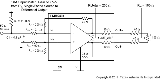
The output considerations remain the same as for the ac-coupled design. Again, the input can be dc coupled when the output is ac coupled. A dc-coupled input with an ac-coupled output can have some advantages to move the input VICM down if the source is ground referenced. When the source is dc coupled into the LMH5401-SP (as shown in Figure 58), both sides of the input circuit must be dc coupled to retain differential balance. Normally, the non-signal input side has an RG element biased to whatever the source midrange is expected to be. Providing this mid-scale reference gives a balanced differential swing around VOCM at the outputs. Often, RG2 is simply grounded for dc-coupled, bipolar-input applications. This configuration gives a balanced differential output if the source swings around ground. If the source swings from ground to some positive voltage, grounding RG2 gives a unipolar output differential swing from both outputs at VOCM (when the input is at ground) to one polarity of swing. Biasing RG2 to an expected midpoint for the input signal creates a differential output swing around VOCM. One significant consideration for a dc-coupled input is that VOCM sets up a common-mode bias current from the output back through RF and RG to the source on both sides of the feedback. Without input-balancing networks, the source must sink or source this dc current. After the input signal range and biasing on the other RG element is set, check that the voltage divider from VOCM to VI through RF and RG (and possibly RS) establishes an input VICM at the device input pins that is in range.
LMH5401-SP 006_SBOS849_SEC9p3p2p2_DC_SEDE.gifFigure 58. DC-Coupled, Single-Ended-to-Differential, Gv = 7 V/V