ZHCSH86B December 2017 – February 2019 LMH5401-SP
PRODUCTION DATA.
- 1 特性
- 2 应用
- 3 说明
- 4 修订历史记录
- 5 说明 (续)
- 6 Pin Configuration and Functions
- 7 Specifications
-
8 Parameter Measurement Information
- 8.1 Output Reference Nodes and Gain Nomenclature
- 8.2 ATE Testing and DC Measurements
- 8.3 Frequency Response
- 8.4 S-Parameters
- 8.5 Frequency Response with Capacitive Load
- 8.6 Distortion
- 8.7 Noise Figure
- 8.8 Pulse Response, Slew Rate, and Overdrive Recovery
- 8.9 Power Down
- 8.10 VCM Frequency Response
- 8.11 Test Schematics
- 9 Detailed Description
-
10Application and Implementation
- 10.1 Application Information
- 10.2
Typical Application
- 10.2.1 Design Requirements
- 10.2.2 Detailed Design Procedure
- 10.2.3 Application Curves
- 10.3 Do's and Don'ts
- 11Power Supply Recommendations
- 12Layout
- 13器件和文档支持
- 14机械、封装和可订购信息
10.2.2.4.4 ADC Input Common-Mode Voltage Considerations—DC-Coupled Input
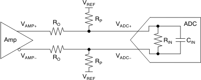
DC-coupled applications vary in complexity and requirements, depending on the ADC. One typical requirement is resolving the mismatch between the common-mode voltage of the driving amplifier and the ADC. Devices such as the ADS5424 require a nominal 2.4-V input common-mode, whereas other devices such as the ADS5485 require a nominal 3.1-V input common-mode; still others such as the ADS6149 and the ADS4149 require 1.5 V and 0.95 V, respectively. As shown in Figure 69, a resistor network can be used to perform a common-mode level shift. This resistor network consists of the amplifier series output resistors and pull-up or pull-down resistors to a reference voltage. This resistor network introduces signal attenuation that may prevent the use of the full-scale input range of the ADC. ADCs with an input common-mode closer to the typical 2.5-V LMH5401-SP output common-mode are easier to dc-couple, and require little or no level shifting.
 Figure 69. Resistor Network to DC Level-Shift Common-Mode Voltage
 For common-mode analysis of the circuit in Figure 69, assume that VAMP± = VCM and VADC± = VCM (the specification for the ADC input common-mode voltage). VREF is chosen to be a voltage within the system higher than VCM (such as the ADC or amplifier analog supply) or ground, depending on whether the voltage must be pulled up or down, respectively; RO is chosen to be a reasonable value, such as 24.9 Ω. With these known values, RP can be found by using Equation 15:

Shifting the common-mode voltage with the resistor network comes at the expense of signal attenuation. Modeling the ADC input as the parallel combination of a resistance (RIN) and capacitance (CIN) using values taken from the ADC data sheet, the approximate differential input impedance (ZIN) for the ADC can be calculated at the signal frequency. The effect of CIN on the overall calculation of gain is typically minimal and can be ignored for simplicity (that is, ZIN = RIN). The ADC input impedance creates a divider with the resistor network; the gain (attenuation) for this divider can be calculated by Equation 16:

With ADCs that have internal resistors that bias the ADC input to the ADC input common-mode voltage, the effective RIN is equal to twice the value of the bias resistor. For example, the ADS5485 has a 1-kΩ resistor tying each input to the ADC VCM; therefore, the effective differential RIN is 2 kΩ.
The introduction of the RP resistors also modifies the effective load that must be driven by the amplifier. Equation 17 shows the effective load created when using the RP resistors.
The RP resistors function in parallel to the ADC input such that the effective load (output current) at the amplifier output is increased. Higher current loads limit the LMH5401-SP differential output swing.
By using the gain and knowing the full-scale input of the ADC (VADC FS), the required amplitude to drive the ADC with the network can be calculated using Equation 18:

As with any design, testing is recommended to validate whether the specific design goals are met.